Microchip MCP3301 Manual


Læs gratis den danske manual til Microchip MCP3301 (6 sider) i kategorien Ikke kategoriseret. Denne vejledning er vurderet som hjælpsom af 12 personer og har en gennemsnitlig bedømmelse på 4.3 stjerner ud af 6.5 anmeldelser. Har du et spørgsmål om Microchip MCP3301, eller vil du spørge andre brugere om produktet?

Side 1/6
2002 Microchip Technology Inc. DS00842A-page 1
MAN842
INTRODUCTION
True differential converters can offer many advantages
over single-ended input A/D Converters (ADC). In addi-
tion to their common mode rejection ability, these con-
verters can also be used to overcome many DC biasing
limitations of common signal conditioning circuits.
Listed below are some typical application issues that
can be solved with proper biasing of a differential con-
verter:
Limited output swing of amplifiers
Unwanted DC-bias point
Low level noise riding on ground
Unwanted or changing common mode level of
input signal
This application note discusses differential input config-
urations and their operation, circuits to implement
these input modes and techniques in choosing the cor-
rect voltage levels to overcome the previously
mentioned challenges.
DIFFERENTIAL AND SINGLE-ENDED
INPUT CONFIGURATIONS
Before discussing biasing solutions, it is important to
understand the functionality of differential A/D convert-
ers. The true differential A/D converter outputs a digital
representation of a differential input signal, typically a
two’s complement binary formatted output. The con-
verter output can be either signed positive or negative,
depending on the voltage level of the differential pair.
The following equation expresses this relationship for
the MCP330X devices:
EQUATION:
The binary output for the MCP330X is a 13-bit output
(12-bit plus sign output).
It is important to note that the converter output is zero
when the inputs are equal. As the voltage difference
between IN+ and IN- increases, the output code also
increases. The maximum voltage at which digital code
saturation will occur is VREF. The differential conver-
sion of the MCP330X converters will reject any DC
common mode signal at the inputs. For the MCP330X
converters, the common mode input range is rail-to-
rail, VSS-0.3V to VDD+0.3V.
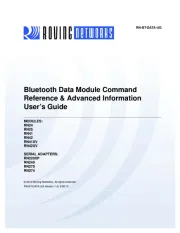
The circuit in Figure 1 shows a differential signal being
applied to the IN+ and IN- pins of the converter. This
method is referred to as full differential operation of the
converter. The graph below the circuit shows possible
voltage levels for a differential application. The inputs
are centered around a common mode voltage, VCM.
VREF is equal to the maximum input swing, shown here
as VDD. By setting V
REF equal to the maximum input
swing of the signal, the full range of the A/D converter
is being used.
FIGURE 1: Driving a true differential
converter with a true differential input.
Author: Craig L. King
Microchip Technology Inc.
Digital Code 2n( ) IN+IN-
( )
2V REF
--------------------------------------=
VDD
1 µF
Input Signal
Differential VREF
p-p
VREF
p-p
VCM
-4096 +4095
Output Code
IN+
IN-
VREF
VDD
1/2VDD
GND
Voltage Levels (V)
VCM
IN+
IN-
VREF VDD
VSS
Differential ADC Biasing Techniques, Tips and Tricks
AN842
DS00842A-page 2 2002 Microchip Technology Inc.
SINGLE-ENDED SIGNALS
Some signals are single-ended, and a true differential
converter can be used in this situation as well. Figure 2
shows a single-ended signal being applied to the IN+
terminal. The common mode voltage is connected to
the negative input of the A/D converter, with the signal
connected to the positive input. This method is referred
to as pseudo-differential operation, with only one of the
inputs being used to obtain a bipolar output of all
codes.
The graph below the circuit in Figure 2 shows that by
setting VREF and IN- to half of the input swing of the sig-
nal, all codes will be present at the output. (The
numbers shown in this example are for a 13-bit
converter).
FIGURE 2: Driving a true differential
converter with a single-ended input to obtain
bipolar output codes.
PSEUDO DIFFERENTIAL BIASING
CIRCUITS FOR SINGLE-ENDED
APPLICATIONS
In most applications, the voltage reference of the ADC
will be the most stable voltage source in the system.
The accuracy of your data acquisition system is no
more accurate than the voltage reference for the con-
verter itself. This same reference should be used as
your DC bias point in pseudo differential systems.
Figure 2 shows that with a single-ended input, the IN-
and VREF need to be near the midscale of the signal
input swing. An example circuit using this approach is
shown in Figure 3. For a signal with a 5Vp-p swing, IN-
and VREF need to be biased at 2.5V.
FIGURE 3: Example of pseudo
differential biasing circuit.
The MCP1525, 2.5V voltage reference was chosen
where no greater than 1% initial accuracy or 50 ppm
tempco is required. This reference voltage is driving
three nodes of the circuit: the VREF for the converter,
the common mode signal of the signal and the DC bias
point of the signal input going into the positive channel
of the A/D converter. With capacitor C1, AC-coupling
VIN, we are effectively blocking any DC component of
the input signal. This allows us to regulate the DC bias
point and match this voltage to the common mode
voltage and A/D voltage reference.
In this case, VREF, IN- and VCM have been adjusted to
appropriate levels, but still limits the effective input
range of the converter. This assumes that the output
swing of the amplifier is ideal (i.e. rail-to-rail). In real
world applications, this output swing will be limited by
tens or hundreds of millivolts, depending on the output
swing of the amplifier.
PSEUDO DIFFERENTIAL BIASING
TIPS & TRICKS
In choosing the correct VREF and IN- levels, the output
swing limitations of the amplifier can be overcome. The
objective is to bring the input range of the ADC away
from both supply rails. To move the ADC input range
away from the upper supply rail, VREF needs to be
slightly less than VDD/2. To move the ADC input range
away from the lower supply rail, IN- needs to be slightly
greater than V
REF. How far away from the supply rails
depends on the output swing of the amplifier. Figure 4
shows this situation graphically.
-4096 +4095
Output Code
IN+
IN-
VREF
VDD
1/2VDD
GND
Voltage Levels (V)
VDD
1 µF
Input Signal
Single-Ended VREF
p-p
IN+
IN- VREF
VDD
VSS
1/2 VDD
VDD
1 µF
MCP601
10 µF 0.1 µF
R4
R3
R1
C1
VIN
-
+
MCP1525
VIN
VOUT
IN+
IN- VREF
MCP330X


Produkt Specifikationer

Mærke: Microchip
Kategori: Ikke kategoriseret
Model: MCP3301

Har du brug for hjælp?

Hvis du har brug for hjælp til Microchip MCP3301 stil et spørgsmål nedenfor, og andre brugere vil svare dig