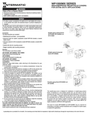
Microchip MIC2800 Manual
Microchip
Ikke kategoriseret
MIC2800
Læs gratis den danske manual til Microchip MIC2800 (70 sider) i kategorien Ikke kategoriseret. Denne vejledning er vurderet som hjælpsom af 14 personer og har en gennemsnitlig bedømmelse på 4.9 stjerner ud af 7.5 anmeldelser. Har du et spørgsmål om Microchip MIC2800, eller vil du spørge andre brugere om produktet?
Side 1/70

SAM9X60-EK
SAM9X60-EK User's Guide
Scope
This user's guide introduces the SAM9X60 Evaluation Kit (SAM9X60-EK) and describes the development and
debugging capabilities running on SAM9 Arm
®-based embedded MPUs.
© 2020 Microchip Technology Inc. User Guide DS50002907B-page 1

Table of Contents
Scope............................................................................................................................................................. 1
1. Introduction............................................................................................................................................. 4
1.1. Document Layout......................................................................................................................... 4
1.2. Recommended Reading...............................................................................................................4
2. Product Overview....................................................................................................................................5
2.1. SAM9X60-EK Features................................................................................................................5
2.2. Evaluation Kit Specifications........................................................................................................ 6
2.3. Power Sources.............................................................................................................................6
2.4. Connectors on Board................................................................................................................... 6
2.5. Default Jumper Settings...............................................................................................................9
2.6. Kit Content....................................................................................................................................9
3. Function Blocks.....................................................................................................................................10
3.1. Power Supply Topology and Power Distribution.........................................................................10
3.2. Processor................................................................................................................................... 14
3.3. On-board Memories................................................................................................................... 29
3.4. Peripherals................................................................................................................................. 33
3.5. User Interaction and Debugging.................................................................................................49
4. Installation and Operation..................................................................................................................... 56
4.1. System and Configuration Requirements...................................................................................56
4.2. Board Setup............................................................................................................................... 56
5. Errata.................................................................................................................................................... 57
5.1. Inoperative LED..........................................................................................................................57
5.2. Booting Issue..............................................................................................................................57
5.3. Powering-Up Issue..................................................................................................................... 57
5.4. Resistor Mislabeling................................................................................................................... 58
6. Appendix. Schematics and Layouts...................................................................................................... 60
7. Revision History.................................................................................................................................... 67
7.1. DS50002907B - 01/2020............................................................................................................67
7.2. DS50002907A - 10/2019............................................................................................................67
The Microchip Website.................................................................................................................................68
Product Change Notification Service............................................................................................................68
Customer Support........................................................................................................................................ 68
Microchip Devices Code Protection Feature................................................................................................68
Legal Notice................................................................................................................................................. 68
Trademarks.................................................................................................................................................. 69
Quality Management System....................................................................................................................... 69
SAM9X60-EK
© 2020 Microchip Technology Inc. User Guide DS50002907B-page 2

Worldwide Sales and Service.......................................................................................................................70
SAM9X60-EK
© 2020 Microchip Technology Inc. User Guide DS50002907B-page 3

1. Introduction
1.1 Document Layout
The document is organized as follows:
• Chapter 1. “Introduction”
• Chapter 2. “Product Overview” – Important information about the SAM9X60-EK board
• Chapter 3. “Function Blocks” – Specifications of the SAM9X60-EK and high-level description of the major
components and interfaces
• Chapter 4. “Installation and Operation” – Instructions on how to get started with the SAM9X60-EK
• Appendix. “Schematics and Layouts” – SAM9X60-EK schematics and layout diagrams
1.2 Recommended Reading
The following Microchip document is available and recommended as a supplemental reference resource:
• SAM9X60 Datasheet. Lit. Number DS60001579
SAM9X60-EK
Introduction
© 2020 Microchip Technology Inc. User Guide DS50002907B-page 4

2. Product Overview
The SAM9X60-EK follows the Microchip MPU strategy for low cost evaluation kits, showcasing all the features that
the SAM9X60 MPU can offer.
2.1 SAM9X60-EK Features
Table 2-1. SAM9X60-EK Features
Characteristic Specification Featured Components
Processor 228-ball TFBGA, 11x11 mm, 0.65 mm pitch Microchip SAM9X60
External clock
MPU: 24 MHz, 32.768 KHz
Misc. osc.: 25 MHz
DSC1001CI5
DSC6083CE2A
Memory
One 16-bit, 2-Gbit DDR2
One NAND Flash
One QSPI Flash
One EEPROM
Winbond W972GG6KB-25
Micron MT29F4G08ABAEA
Microchip SST26VF064B
Microchip 24AA02E48
SD/MMC One standard 4-bit SD card interface –
USB
Two stacked Type-A connectors with power
switches
One Micro-B USB Device
2 * Microchip MIC2025
CAN Two CAN interfaces Microchip MCP2542
Ethernet One ETH port Microchip KSZ8081
Wi-Fi/BT One optional Wi-Fi® /Bluetooth® interface Slot for Microchip ATWILC3000
Audio One ClassD audio port –
Display One 24-bit LCD interface –
Camera One 12-bit Image Sensor Interface –
IO One expander IO Microchip MCP23008
Debug port
One J-Link-OB + CDC
One JTAG interface
Embedded J-Link-OB through the CDC
interface (ATSAM3U4C TFBGA100)
Board monitor
One RGB (Red, Green, Blue) LED
Four push button switches
–
–
Expansion
One PIO connector
One mikroBUS™ connector
–
Hundreds of possible Click™ extensions
featuring Microchip functions inside
Power management
Two power regulators
Two power consumption measurement devices
Microchip MIC2800, MCP1725
Microchip PAC1934, PAC1710
Board supply From USB A or from external connector –
Backup battery SuperCap –
SAM9X60-EK
Product Overview
© 2020 Microchip Technology Inc. User Guide DS50002907B-page 5

2.2 Evaluation Kit Specifications
Table 2-2. Evaluation Kit Specifications
Characteristic Specification
Board SAM9X60-EK
Board supply voltage External or USB-powered
Temperature Operating: 0°C to +70°C
Storage: –40°C to +85°C
Relative humidity 0 to 90% (non-condensing)
Main board dimensions 150 × 125 × 20 mm
RoHS status Compliant
Board identification SAM9X60 Evaluation Kit
2.3 Power Sources
Two options are available to power up the SAM9X60-EK board:
• Powering through an external AC to DC +5V wall adapter connector (J1)
• Powering through the USB Micro-B connector on the USBA port (J7 – default choice)
Table 2-3. Electrical Characteristics
Electrical Parameters Value
Input voltage 5VDC
Maximum input voltage (limits) 6VDC
Maximum 3.3VDC current 300 mA
CAUTION
The SAM9X60-EK board runs at a 3.3V voltage level logic. The maximum voltage that the I/O pins can
tolerate is 3.3V. Providing higher voltages (e.g., 5V) to an I/O pin could damage the board.
2.4 Connectors on Board
The fully-featured SAM9X60-EK board integrates multiple peripherals and interface connectors, as shown in the
following figures.
SAM9X60-EK
Product Overview
© 2020 Microchip Technology Inc. User Guide DS50002907B-page 6

Figure 2-1. SAM9X60-EK Top Connectors
D1
J8
J1
Q5
Q1 R9
R249 R245
R236
R242
R8
R34
R48
R49
FB6
C113
R153
D7
C69
C77
J2
C85 D2
C88
R128 R91
Y6
C56
C128
C126
R171 R181
J16
R19
R18
VDD_3V3_3U
C150 U27
R116
C120
Q12
R114
C117
R149
C90
R221
TP4 R225 R224
R231R230
R218
TP6
R213
C127
VBUS_USBC
Q3
R16
C173
Y10
C152
R235
R238
C2
R10
C6
L1
R7
R250
C176
J7
C4
U6
C122
R94
R93
R84
C58
C116
Q10
Q11
J5
Y2
SW1
R156
R158
R74
R72
SW2
R53
R54
R45
R41
R32
R67
R62
SW3
R97
R98C54
C136
Y8
R162
R110
R111
R109
Y7
C131
D4
R177
C141
C99
J14 FB13
J22
J24
C8
C172
R251
R237
D8
FB1
U1 R11
R29
C18
C1
C19
R246 R234
C148
R239
R258
R256
U2
C5
R4
R13
R12
U4
R243
R233
R241
R257
R47
R36
R35 U9
R265
FB8
C119
R92
R90
C60
R189
J3
R155
U10
J20
C76
C70
Y3
R188
J13
R126
C86
U11
R27
R28
Y1
R197
D3 R20
R119
U5
R22
R24
R21 C27
C25
C23
Y5
C91
R88
R86
R159
R157
U8
R85
R82
R75
R71
R65
R66
R203
R201
R199
Q15
Q14
Q13
U21
C125
C129
C55
U26
R59
R52
R145
R44
R40
R31
R142
R68
R64
R196
U7
R191
R185
J17
R136
R175
J9
R118
R107
C57
R112
R108
R113
C100
R137
R172
FB9
R161
R138 Q7
Q6
D5
J11
R173
R170
R169
Q9
Q8
R174
R182
D6
U24
Y9
U28
R17
Q2
TP9 C149
R1
R6
C106
VDDIOM
C61
VDD_3V3
U32
R117
U20
C124
C123
C121
U19
C118
C115
C114
R187
TP2
R127
R122
R220 R223R222
C92
C93
R215
R216 R219
R227
R229
R226
R228
U23
TP5
TP7
R26
R190
C105
U17
U15
C103 C97
U14
C104
C102
C101
C130
R160
R176
FB10
C142
C138
R179R178
FB11
C137
R183
R180
VDDCOREVBUS_USBA
VBUS_USBB
C9
C3
C20
C22
C7
R148
R150
R33
C12
C11
D9
R132
R133
R79
R80
C29
SW4
R195
R58
R141
R146
U13
U12 C95
C132
R5
R2
Q4
C17
VBUS_JLINK
C171
C151
J18
U3 R96
R95
R154
R89
R87
R37
C179
R259 R260
J19
R130
R124
R152
R81
R77
R69
C75
C62
R70
C24
R194
J21
LD1
VDD_WILC
R207 R202
R105
R104
R135
R134
J6
J10
U22 C134
C133
R139
J12
R3
R15
R240
J23
R83
C53
C59
U31
R115
R123
C26
R212
C96
TP8
C135
J4
U16
VDD_MAIN_5V
Configuration
Jumpers ISI
Connector
2 x CAN
Connector
CLASSD Audio
Connector
JTAG 20-pin
IDC Connector
UART
DEBUG
JLINK USB
Micro-B
External
Power Jack
MikroBus
USB 2.0
Micro-B
Stacked USB
type A
Ethernet
10/100 4 x User Buttons I2C and PCM audio header
to/from ATWILC3000
Place to solder the
Wi-Fi / BT Module
SD Card
Connector
Raspberry Pi
Connector
™
SAM9X60-EK
Product Overview
© 2020 Microchip Technology Inc. User Guide DS50002907B-page 7

...........continued
Connector Interfaces to
J5 Ethernet 10/100 RJ45 (port 1)
J11 Audio external power
J12 ClassD audio output
J14 mikroBUS socket
J15 LCD connector
J16 External GPIO
J17 ISI Camera Connector
J18 PCB connector for factory-programming the SAM3U/J-Link-OB (not to be used by end user)
J22 USB 2.0 Micro-B, J-Link-OB/J-Link-CDC
J23 JTAG, 20-pin IDC
J24 FTDI connector (UART debugger)
2.5 Default Jumper Settings
Table 2-5. SAM9X60-EK Jumper Settings
Jumper State Function
J2 Closed VDDBU current measurement
J3
Closed Disable the SHDN function and always keep the board powered on
Open (default) Normal behavior, the PMIC can be powered down by the MPU
J13 Closed Booting from on-board memories is permanently disabled
Open (default) Booting from on-board memories is disabled only when SW4 is pressed
J19
(not populated)
Closed Erase SAM3U firmware (not populated, reserved for factory configuration and
should never be used by the end user)
Open (default) Normal SAM3U operation (runs the J-Link interface)
J20
Closed J-Link on-board interface is disabled. MPU debugging is done through J23, the 20-
pin SAM-ICE™ connector (i.e., an external JTAG interface is required)
Open (default) J-Link on-board interface is enabled. MPU debugging is done through it (i.e., using
the SAM3U MCU and the micro USB connector J22)
J21
Closed Disable UART communication (CDC) between MPU and SAM3U
Open (default) Enable UART communication (CDC) between MPU and SAM3U (PD20 port must
be high as well)
2.6 Kit Content
The SAM9X60 evaluation kit includes the following:
• The SAM9X60-EK board
• USB-A to USB Micro-B cable
• 50-position FFC/FPC cable
SAM9X60-EK
Product Overview
© 2020 Microchip Technology Inc. User Guide DS50002907B-page 9

The switch between the two powering options is made by four transistors that ensure the separation between the two
when both are plugged. The switch prioritizes powering from the wall adapter to maximize power transfer.
The following figure shows the input power supply topology.
Figure 3-2. Input Power Options
0.1uF
50V
0402
C3
0.1uF
50V
0402
C9
GND
IN
1
IN_PAD
7
EN
6
GND
2FLAG 3
OUT2 5
OUT1 4
NCP349MNAETBG
U1
2
3
1
2.1mm
EJ508A
J1
VDD_MAIN_5V_
GND
EXT_5V DC_5V
180R 0603
FB1 USB_5V
0.1uF
50V
0402
C7
2
71
6
SIA923AEDJ-T1-GE3
Q1A
5
8 4
3
SIA923AEDJ-T1-GE3
Q1B
2
71
6
SIA923AEDJ-T1-GE3
Q2A
5
8 4
3
SIA923AEDJ-T1-GE3
Q2B
GND GND GND GND
GND GND GND
100 Fµ
16V
Radial, Can
C4
GND
USBA_VBUS_5V
10uF
25V
1206
C1
10uF
25V
1206
C2
10uF
25V
1206
C8
100k
0402
5%
R2
100k
0402
5%
R3
100k
0402
5%
R5
Note: USB-powered operation eliminates additional wires and batteries. It is the preferred mode of operation for any
project that requires only a 5V source at up to 500 mA.
3.1.2 Power Management Integrated Circuit
The MIC2800 is a high-performance power management IC providing three output voltages with maximum efficiency.
Integrating a 2-MHz DC/DC converter with an LDO post-regulator, the MIC2800 gives two high-efficiency outputs with
a second, 300 mA LDO for maximum flexibility. The DC-to-DC converter uses small values of L and C to reduce
board space while still retaining efficiency over 90% at load currents up to 600 mA. For more information about the
MIC2800, refer to the product .web page
Each LDO has an independent Enable (EN) pin thus allowing a proper power-up sequence for the MPU. The 20 KΩ
resistor in series and the 0.1 µF capacitor in parallel with the EN1 input make a low-pass filter and introduce the
necessary delay between the 3.3V and 1.15V rails needed for the proper operation of the MPU. The diode (D1 in
Figure 3-3) ensures that the capacitor fast discharges during the power-down sequence.
Detailed information on the SAM9X60 MPU power supplies and power-up/down considerations are described in
section “Electrical Characteristics” in the SAM9X60 device datasheet (see ).1.2 Recommended Reading
The MIC2800-G8S comes preset to supply all the voltage rails needed by the system:
• 1.8V DC/DC supplies SAM9X60 DDR2 pads (VDDIOM) and devices.
• 1.15V LDO1 supplies SAM9X60 Core (VDDCORE).
• 3.3V LDO2 supplies SAM9X60 I/O pads.
The figure below shows the power management scheme.
SAM9X60-EK
Function Blocks
© 2020 Microchip Technology Inc. User Guide DS50002907B-page 11

Figure 3-3. Power Management Integrated Circuit
GND GNDGND GND
VDD_1V15
VDD_MAIN_5V
2.2uH
L1
GND
GNDGND
VDD_1V8
GND
GND
GND
MIC2800_nRST
GND
0.1uF
50V
0402
C17
0.1uF
50V
0402
C18
0.1uF
50V
0402
C19
LOWQ
1
BIAS
2
SGND 3
PGND
4
SW 5
VIN
6
VIN
7
LDO2 8
FB 9
LDO 10
LDO1 11
POR 12
CSET 13
CBYP
14
EN1
15
EN2
16
U3
MIC2800-G8SYML-TR
600mA
300mA
300mA
VDD_3V3_LDO
POWER_EN
10uF
25V
1206
C10
10uF
25V
1206
C11
10uF
25V
1206
C12
10uF
25V
1206
C21
10uF
25V
1206
C22
10nF
16V
0402
C20
1N4148
D1
20k 0402 1%
R11
100k
0402
5%
R29
3.1.3 Shutdown Circuitry
The processor can assert the SHDN signal to shut down the PMIC and enter Power-down mode. This is done by
pulling both enable pins of the PMIC to GND through a Field Effect Transistor (FET) scheme.
Jumper J3 must not be set to enable this functionality. By setting jumper JP2/J3, the user can shut down the MPU
without powering down its power rails.
Figure 3-4. Shutdown Circuitry
10k
0402
5%
R19
1k
0402
5%
R18
12
HDR-2.54 Male 1x2
J3
GND GND GND
VDD_MAIN_5V VDD_MAIN_5V
SHDN
POWER_EN
Shunt 2.54mm 1x2
JP2
GND
MIC2800_nRST
STARTB
VDD_3V3
100k
0402
5%
R15
100k
0402
5%
R16
100k
0402
5%
R17
3
1
2
BSS138N
Q3
3
1
2
BSS138N
Q4
3
1
2
BSS138N
Q5
3.1.4 Battery Unit
A 3.3V battery (supercapacitor) is implemented to permanently maintain the VDDBU voltage.
This function allows the user to shut down the MPU and the system, thus entering a low power mode, and still keep
the custom configuration that was previously set in the MPU backup area. While in Shut-down mode, the board can
be woken up by action on the SW2 button (WAKE UP), which signals the MPU to resume operations.
Jumper JP1/J2 must be in place for proper operation of the MPU, and can be removed if the user wants to bring the
MPU back to the initial configuration, by resetting the General Purpose Backup Registers (GPBR).
WARNING
Make sure the board is powered off before removing the JP1/J2 jumper.
SAM9X60-EK
Function Blocks
© 2020 Microchip Technology Inc. User Guide DS50002907B-page 12

Figure 3-5. Battery Unit
220mF
3.3V
P8.3L11.7D6.8H1.8
C23
1
2
3
BAT54C
D2
PMEG6010ER
D3
VDDBU
GND
Shunt 2.54mm 1x2
JP1
VDD_3V3
12
HDR-2.54 Male 1x2
J2
100R
0402
1%
R20
3.1.5 Current Measurement
Two Microchip DC power/energy monitors are embedded on the SAM9X60-EK board:
• one single high-side current sense monitor PAC1710
• one four-channel current sense monitor PAC1934
Both chips communicate with the MPU via a Two-wire Interface (TWI) and both output their ALERT# signal to a port
expander.
The PAC1710 is a single high-side bidirectional current sensing monitor with precision voltage measurement
capabilities. The power monitor measures the voltage developed across an external sense resistor to represent the
high-side current of a battery or voltage regulator. The PAC1710 also measures the SENSE+ pin voltage and
calculates average power over the integration period. The PAC1710 can be programmed to assert the ALERT# pin
when high and low limits are exceeded for current sense and bus voltage. For more information about the PAC1710,
refer to the product .web page
One current sense resistor is populated on board for measuring voltage and current on the main 5V power rail.
Figure 3-6. PAC1710 Current Measurement
I2C ADR : 1001_101[R/W]
GND GND GND
10k
0402
5%
R4
VDD_3V3
VDD_MAIN_5V_ VDD_MAIN_5V
PAC1710_TWCK
PAC1710_TWD
VDD_MAIN_5V
GND
PAC1710_INT
1 2
3
4
0.01R
1206
1%
0.25W
R1
SENSE+ 1
SENSE- 2
NC 3
NC 4
GND
5ADDR_SEL 6
ALERT# 7
SMDAT A 8
SMCLK 9
VDD
10
PAD
11
PAC1710
U2
5V_P 5V_N
TP LOOP Black TH
TP1
4.7uF
10V
0402
C5
0.1uF
50V
0402
C6
VDD_3V3_LDO
100R
0402
1%
R6
Table 3-1. PAC1710 Signal Descriptions
PIO Signal Name Shared PIO Signal Description
PA31 PAC1710_TWCK Power TWI TWI clock
PA30 PAC1710_TWD Power TWI TWI data
– PAC1710_INT – Interrupt – to port expander U6
The PAC1934 is a four-channel power/energy monitor with current sensor amplifier and bus voltage monitors that
feed high resolution ADCs. Digital circuitry performs power calculations and energy accumulation. The PAC1934
enables energy monitoring with integration periods from 1 ms to up to 36 hours. Bus voltage, sense resistor voltage,
and accumulated proportional power are stored in registers for retrieval by the system master or embedded
controller. For more information about the PAC1934, refer to the product .web page
SAM9X60-EK
Function Blocks
© 2020 Microchip Technology Inc. User Guide DS50002907B-page 13

Figure 3-8. Processor Power Supplies
GND
0.1uF16V0201 C32
0.1uF16V0201 C33
4.7uF10V0402 C31
VDDCORE
L6
VDDCORE
F6
VDDCORE
F11
VDDIOM
G14
VDDIOM
C10
VDDIOM
C13
VDDANA
C4
VDDIN33
P13
VDDOUT25
P10
VDDIN33
L11
GND J8
GND E7
GND G12
GNDANA B4
GNDIN33 R13
VDDNF
K14
VDDIOP0
G3
GND E10
GND B13
GND K5
GND G5
GND N15
VDDQSPI
C7
VDDIOP0
K3
GND H8
GND H9
GNDIN33 M10
GND K12
GND T16
GND A1
GND A16
GND T1
VDDBU
P7 GND M7
VDDIOP1
N3 GND N2
U5G
SAM9X6_TFBGA-228
VDDOUT25
VDDBU
VDDCORE
VDDIOM
0.1uF16V0201 C34
0.1uF16V0201 C36
0.1uF16V0201 C37
0.1uF16V0201 C38
0.1uF16V0201 C41
0.1uF16V0201 C42
0.1uF16V0201 C43
0.1uF16V0201 C44
0.1uF16V0201 C45
0.1uF16V0201 C46
0.1uF16V0201 C48
0.1uF16V0201 C49
4.7uF10V0402 C47
0.1uF16V0201 C50
0.1uF16V0201 C51
GND
4.7uF10V0402 C35
VDDIN33
VDDIN33
2.2uF10V0402 C52
4.7uF10V0402 C40
4.7uF10V0402 C39
0R 2040
R30
VDD_3V3_MPU
VDD_3V3_MPU
3.2.2 Main Configuration and Control
This block depicts the main block for processor configuration and control:
• XIN and XOUT are the Main Clock Oscillator input/output.
• XIN32 and XOUT32 are the Slow Clock Oscillator input/output.
• SHDN is an output signal used to enable and disable an external power supply circuit.
• WKUP is an event detection input pin used to wake up the processor from Shutdown state.
• JTAGSEL is an input that when pulled high enables the JTAG boundary scan.
• TCK, TDI, TDO, TMS and RTCK are used for JTAG communication.
• nRST is the processor main reset input.
• HHSD_A/B/C are the three USB ports embedded inside the MPU.
• RTUNE is used for USB external tuning.
• TST input is reserved for processor manufacturing tests.
• ADVREFP and ADVREFN are the positive and negative reference points for the embedded analog comparator.
A small low-pass filter is placed to reduce the input noise and improve accuracy.
SAM9X60-EK
Function Blocks
© 2020 Microchip Technology Inc. User Guide DS50002907B-page 15

3.2.4 Reset Circuitry
Three reset sources for the SAM9X60 MPU are placed on the board:
• Power-on Reset from the power management unit MIC2800
• User push button reset SW3
• External JTAG or J-Link-OB reset from an in-circuit emulator
Figure 3-11. Processor Reset Circuitry
MIC2800_nRST
JTAG_nRST
100R 04021%
R185
100R 04021%
R190
100R 04021%
R191
USER_nRST MPU_nRST
3.2.5 DDR Controller (MPDDRC)
The SAM9X60 embeds a Multi-Port DDR-SDRAM Controller (MPDDRC) to drive DDR2 and LPDDR1 memories.
Note the following regarding the command and control signal connections between the DDR Controller and the DDR
Memory:
• Addresses A0, A1 and A12 are not used on the controller side.
• Addresses A2 to A11 are connected to A0 to A9 on the memory side.
• Signal SDA10 must be connected to A10.
• Addresses A13 to A15 are connected to the last three addresses on the memory side.
• A16 to A18 are connected to BA0 to BA2.
It is recommended to double-check the design schematic against the information provided in the datasheet.
Figure 3-12. Processor DDR Controller
DDR_A2
DDR_A3
DDR_A4
DDR_A5
DDR_A6
DDR_A7
DDR_A8
DDR_A9
DDR_A10
DDR_A11
DDR_A13
DDR_A14
DDR_A15
DDR_D3
DDR_D6
DDR_D4
DDR_D1
DDR_D5
DDR_D2
DDR_D7
DDR_D0
DDR_D12
DDR_D15
DDR_D13
DDR_D8
DDR_D9
DDR_D10
DDR_D14
DDR_D11
DDR_DQM0
DDR_DQM1
DDR_DQS0_P
DDR_DQS0_N
DDR_DQS1_P
DDR_DQS1_N
DDR_RAS
DDR_CAS
DDR_WE
DDR_CS
DDR_CLK_P
DDR_CLK_N
DDR_CKE
22pF
50V
0402
C62
DDR_A16
DDR_A17
DDR_A18
20k
0402
1%
R119
GND
DDR_SDA10
DIFF100
DIFF100
DIFF100
DIFF100
DIFF100
DIFF100
SDCKn
B14 SDCK
A15
SDCKE
F13
nWR0
E8
SDA10
D12
nRD
F12
nWR1
A10
DDR_CAL
B8
A1
G16
A15
G15
A8
F16
A4
B12
A0
B10
A13
B11
A10
C11
A6
A12
A2
A13
A17
F14
A12
A11
A19
H14
A16
E14
A18
C16
A3
D15
A7
B16
A5
E11
A14
C15
A9
D14
A11
E13 D10 F9
D9 D8
D13 B9
D14 D11
D6 J16
D11 A9
D8 G9
D12 F10
D3 H11
D4 J14
D1 H10
D7 J13
D0 H16
D2 H15
D5 J11
D15 C9
DDR_VREF A14
nCS1 E16
nCS0 F15
DQS1 D9
SDWE D16
nDQS1 E9
RAS E15
nDQS0 H13
DQS0 H12
CAS C12
DQM1 C8
DQM0 G11
nWR3
L14
U5E
SAM9X6_TFBGA-228
DDR_VREF
SAM9X60-EK
Function Blocks
© 2020 Microchip Technology Inc. User Guide DS50002907B-page 17

Figure 3-15. Processor PIOs PB and PD
LCD_IRQ2_PB17
ETH0_TXCK_PB04
ETH0_TX0_PB09
ETH0_TXEN_PB07
ETH0_TX1_PB10
ETH0_RX1_PB01
ETH0_RX0_PB00
ETH0_RXER_PB02
ETH0_RXDV_PB03
ETH0_MDC_PB06
ETH0_MDIO_PB05
ETH0_IRQ_PB08
NAND_IO0_PD06
NAND_IO1_PD07
NAND_IO2_PD08
NAND_IO3_PD09
NAND_IO4_PD10
NAND_IO5_PD11
NAND_IO6_PD12
NAND_IO7_PD13
NAND_CLE_PD03
NAND_ALE_PD02
NAND_nWE_PD01
NAND_nRE_PD00
NAND_nCS_PD04
NAND_RB_PD05
USBB_EN_5V_PD15
USBC_EN_5V_PD16
MBUS_AD4_PB15
USBA_VBUSDETECT_PB16
MBUS_RST_PB14
NRST_PB25
SEL_FNCT1_PD19
SEL_FNCT2_PD20
MCP23008_INT_PD17
PB19
PB20
PB21
PB22
PB23
PB24
MBUS_INT_PB18
PB11
PB12
PB13
CAN_STBY_PD21
LCD_ID_PD14
USER_BUTTON_PD18
PB0 F4
PB1 C1
PB2 D3
PB3 D1
PB4 E3
PB5 E1
PB6 D2
PB7 A5
PB8 E6
PB9 A2
PB10 A3
PB11 D6
PB12 C2
PB13 A4
PB14 F2
PB15 B5
PB16 B3
PB17 B1
PB18 E4
PB19 C6
PB20 A6
PB21 A7
PB22 B7
PB23 B6
PB24 A8
PB25 E2
U5B
SAM9X6_TFBGA-228
PD0 R14
PD1 T15
PD2 P15
PD3 N14
PD4 R16
PD5 N11
PD6 K16
PD7 J12
PD8 K15
PD9 J10
PD10 L16
PD11 K11
PD12 L15
PD13 J15
PD14 L12
PD15 M16
PD16 M14
PD17 N16
PD18 L13
PD19 P16
PD20 M11
PD21 M15
U5D
SAM9X6_TFBGA-228
Some of the ports were multiplexed to accommodate more devices on the evaluation kit and to showcase all the
functions the SAM9X60 MPU can address off a single PIO wire.
Most of the ports that share multiple functions are split through passive resistors placed on the board as close to the
MPU as possible, therefore no other hardware change must be made. In most cases, the user can use only one of
their functions at a time, or can develop a composite driver enabling the use of multiple functions at the same time.
Figure 3-16. Processor PIO Muxing
22R 0402 1%
R31
22R 0402 1%
R32
22R 0402 1%
R38
22R 0402 1%
R39
22R 0402 1%
R40
22R 0402 1%
R41 SDMMC1_WILC3000_DAT3_PA04
SDMMC1_WILC3000_DAT2_PA03
SDMMC1_WILC3000_DAT1_PA02
SDMMC1_WILC3000_DAT0_PA11
SDMMC1_WILC3000_CMD_PA12
SDMMC1_WILC3000_CK_PA13
FLEXCOM5_IO4_BT_RTS_PA07
FLEXCOM5_IO3_BT_CTS_PA08
PA02
PA03
PA04
PA07
PA08
PA11
PA12
PA13
PA14
22R 0402 1%
R42
22R 0402 1%
R43
22R 0402 1%
R44
22R 0402 1%
R45
22R 0402 1%
R46
22R 0402 1%
R50
22R 0402 1%
R51
22R 0402 1%
R52
22R 0402 1%
R53
22R 0402 1%
R54
22R 0402 1%
R55
22R 0402 1%
R56
22R 0402 1%
R57
22R 0402 1%
R58
22R 0402 1%
R59
EXT40_GPIO_PA02
EXT40_GPIO_PA03
EXT40_GPIO_PA04
EXT40_SPI_MOSI_PA12
EXT40_SPI_MISO_PA11
EXT40_SPI_SCLK_PA13
EXT40_GPIO_PA14
EXT40_NPCS1_PA07
EXT40_NPCS2_PA08
MBUS_NPCS0_PA14
MBUS_SPCK_PA13
MBUS_MISO_PA11
MBUS_MOSI_PA12
QSPI_IO0_PB21
QSPI_IO1_PB22
QSPI_IO2_PB23
QSPI_IO3_PB24
QSPI_SCK_PB19
QSPI_CS_PB20
22R 0402 1%
R69
22R 0402 1%
R70
22R 0402 1%
R71
22R 0402 1%
R72
PB19
PB20
PB21
22R 0402 1%
R74
22R 0402 1%
R75
22R 0402 1%
R77
22R 0402 1%
R79
22R 0402 1%
R80
22R 0402 1%
R81
PB22
PB23
PB24
PC31
EXT40_I2SMCK_PB23
EXT40_CLK1_PC31
EXT40_I2SWS_PB20
EXT40_I2SCK_PB19
EXT40_GPIO_PB24
EXT40_I2SDIN_PB21
EXT40_I2SDOUT_PB22
ETH0_PCK1_PC31
LED_RED_PB11
LED_GREEN_PB12
LED_BLUE_PB13
EXT40_CLK2_PB13
EXT40_PWM1_PB12
EXT40_PWM0_PB11
0R 0402
R66
0R 0402
R63
0R 0402
R60
PB11
PB12
PB13
MBUS_PWM_PB13
0R 0402
R65
22R 0402 1%
R82
22R 0402 1%
R85
22R 0402 1%
R86
22R 0402 1%
R88
Table 3-3. Processor PIOs Pin Assignment and Signal Description
Pad Power Rail Function I/O Type
PA0 VDDIOP0 (3.3V) FLEXCOM0_IO0 TWI Data (TWD) bidirectional line shared between the LCD,
EEPROMs and external 40-pin header
PA1 VDDIOP0 (3.3V) FLEXCOM0_IO1 TWI Clock (TWCK) output line shared between the LCD, EEPROMs
and external 40-pin header
SAM9X60-EK
Function Blocks
© 2020 Microchip Technology Inc. User Guide DS50002907B-page 19

...........continued
Pad Power Rail Function I/O Type
PA2 VDDIOP0 (3.3V)
SDMMC1_DAT1 SDIO Data 1 (I/O1) bidirectional line for the ATWILC3000 Wi-Fi/BT
module
GPIO GPIO going to the external 40-pin header
PA3 VDDIOP0 (3.3V)
FLEXCOM0_IO3 SDIO Data 2 (I/O2) bidirectional line for the ATWILC3000 Wi-Fi/BT
module
GPIO GPIO going to the external 40-pin header
PA4 VDDIOP0 (3.3V)
FLEXCOM0_IO2 SDIO Data 3 (I/O3) bidirectional line for the ATWILC3000 Wi-Fi/BT
module
GPIO GPIO going to the external 40-pin header
PA5 1VDDIOP0 (3.3V)
FLEXCOM1_IO0 UART Transmit (TX) output line going to the external 40-pin header
CANTX1 CAN Transmit (CANTX) output line going to the second CAN
transceiver MCP2542
PA6 1VDDIOP0 (3.3V)
FLEXCOM1_IO1 UART Receive (RX) input line going to the external 40-pin header
CANRX1 CAN Receive (CANRX) input line going to the second CAN
transceiver MCP2542
PA7 VDDIOP0 (3.3V)
FLEXCOM4_IO4 First SPI Chip Select (nCS) output line for the external 40-pin header
FLEXCOM5_IO4 SPI Request to Send (RTS) output line for the BT module
PA8 VDDIOP0 (3.3V)
FLEXCOM4_IO5 Second SPI Chip Select (nCS) output line for the external 40-pin
header
FLEXCOM5_IO3 SPI Clear to Send (CTS) input line for the BT module
PA9 2VDDIOP0 (3.3V)
DRXD DEBUG UART Receive (DRX) input line
CANRX0 CAN Receive (CANRX) input line going to the first CAN transceiver
MCP2542
PA10 2VDDIOP0 (3.3V)
DTXD DEBUG UART Transmit (DTX) input line
CANTX0 CAN Transmit (CANTX) output line going to the first CAN transceiver
MCP2542
PA11 VDDIOP0 (3.3V)
FLEXCOM4_IO1 SPI Master Input Slave Output (MISO) input line shared between the
mikroBUS and external 40-pin connectors
SDMMC1_DAT0 SDIO Data 0 (I/O0) bidirectional line going to the ATWILC3000 Wi-
Fi/BT module
PA12 VDDIOP0 (3.3V)
FLEXCOM4_IO0 SPI Master Output Slave Input (MOSI) output line shared between the
mikroBUS and external 40-pin connectors
SDMMC1_CMD SDIO Command (CMD) bidirectional line going to the ATWILC3000
Wi-Fi/BT module
PA13 VDDIOP0 (3.3V)
FLEXCOM4_IO2 SPI Source Clock (SCLK) output line shared between the mikroBUS
and external 40-pin connectors
SDMMC1_CK SDIO Data 0 (I/O0) bidirectional line going to the ATWILC3000 Wi-
Fi/BT module
PA14 VDDIOP0 (3.3V)
FLEXCOM4_IO3 SPI Chip Select (nCS) output line for the mikroBUS connector
GPIO GPIO going to the external 40-pin header
SAM9X60-EK
Function Blocks
© 2020 Microchip Technology Inc. User Guide DS50002907B-page 20

...........continued
Pad Power Rail Function I/O Type
PA15 VDDIOP0 (3.3V) SDMMC0_DAT0 SDIO Data 0 (I/O0) bidirectional line going to the SD card connector
PA16 VDDIOP0 (3.3V) SDMMC0_CMD SDIO Command (CMD) bidirectional line going to the SD card
connector
PA17 VDDIOP0 (3.3V) SDMMC0_CK SDIO Clock (CLK) output line going to the SD card connector
PA18 VDDIOP0 (3.3V) SDMMC0_DAT1 SDIO Data 1 (I/O1) bidirectional line going to the SD card connector
PA19 VDDIOP0 (3.3V) SDMMC0_DAT2 SDIO Data 2 (I/O2) bidirectional line going to the SD card connector
PA20 VDDIOP0 (3.3V) SDMMC0_DAT3 SDIO Data 3 (I/O3) bidirectional line going to the SD card connector
PA21 VDDIOP0 (3.3V) FLEXCOM5_IO1 UART Receive (RX) input line shared between the mikroBUS
connector and the BT transceiver on the ATWILC3000 module
PA22 VDDIOP0 (3.3V) FLEXCOM5_IO0 UART Transmit (TX) output line shared between the mikroBUS
connector and the BT transceiver on the ATWILC3000 module
PA23 VDDIOP0 (3.3V) GPIO GPIO used as input to detect when an SD card has been inserted in
the SD connector
PA24 VDDIOP0 (3.3V) CLASSD_L0 CLASSD Left Output L0
PA25 VDDIOP0 (3.3V) CLASSD_L1 CLASSD Left Output L1
PA26 VDDIOP0 (3.3V) CLASSD_L2 CLASSD Left Output L2
PA27 VDDIOP0 (3.3V) CLASSD_L3 CLASSD Left Output L3
PA28 VDDIOP0 (3.3V) GPIO / WKUP4 GPIO Input used to signal any interrupt coming from the WILC300 Wi-
Fi/BT module
PA29 VDDIOP0 (3.3V) GPIO GPIO Output used to enable the WILC300 Wi-Fi/BT module by
enabling its power supply
PA30 VDDIOP0 (3.3V) FLEXCOM6_IO0 TWI Data (TWD) bidirectional signal shared between PAC1934,
PAC1710, MPC23008 and the mikroBUS connector
PA31 VDDIOP0 (3.3V) FLEXCOM6_IO1 TWI Clock (TWCK) Bidirectional signal shared between PAC1934,
PAC1710, MPC23008 and the mikroBUS connector
PB0 VDDANA (3.3V) E0_RX0 RMII Ethernet Receive Data 0 signal going to KSZ8081
PB1 VDDANA (3.3V) E0_RX1 RMII Ethernet Receive Data 1 signal going to KSZ8081
PB2 VDDANA (3.3V) E0_RXER RMII Ethernet Receive Error signal going to KSZ8081
PB3 VDDANA (3.3V) E0_RXDV RMII Ethernet Receive Data Valid signal going to KSZ8081
PB4 VDDANA (3.3V) E0_TXCK RMII Ethernet Transmit Clock signal going to KSZ8081
PB5 VDDANA (3.3V) E0_MDIO RMII Ethernet Management Data I/O signal going to KSZ8081
PB6 VDDANA (3.3V) E0_MDC RMII Ethernet Management Data Clock signal going to KSZ8081
PB7 VDDANA (3.3V) E0_TXEN RMII Ethernet Receive Data Valid signal going to KSZ8081
PB8 VDDANA (3.3V) E0_TXER RMII Ethernet Transmit Coding Error signal going to KSZ8081
PB9 VDDANA (3.3V) E0_TX0 RMII Ethernet Transmit Data 0 signal going to KSZ8081
PB10 VDDANA (3.3V) E0_TX1 RMII Ethernet Transmit Data 1 signal going to KSZ8081
PB11 VDDANA (3.3V) PWM0 PWM signal shared between the LD1 red LED and the 40-pin
connector
SAM9X60-EK
Function Blocks
© 2020 Microchip Technology Inc. User Guide DS50002907B-page 21

...........continued
Pad Power Rail Function I/O Type
PB12 VDDANA (3.3V) PWM1 PWM signal shared between the LD1 green LED and the 40-pin
connector
PB13 VDDANA (3.3V) PWM2 PWM signal shared between the LD1 blue LED, the mikroBUS and
the 40-pin connectors
PB14 VDDANA (3.3V) GPIO GPIO output used as the reset signal for the mikroBUS connector
PB15 VDDANA (3.3V) AD4 Analog input for the mikroBUS connector
PB16 VDDANA (3.3V) GPIO GPIO input used to detect if the board has been connected to a host
on the USBA port
PB17 VDDANA (3.3V) GPIO GPIO input used to signal any interrupt request from the LCD
PB18 VDDANA (3.3V) GPIO GPIO input used to signal any interrupt request from the mikroBUS
connector
PB19 VDDQSPI (3.3V)
QSCK QSPI Serial Clock (SCK) signal going to SST26VF064B
I2SMCC_CK I2S Bit Clock (CK) signal going to the 40-pin connector
PB20 VDDQSPI (3.3V)
QCS QSPI Chip Select (CS) signal going to SST26VF064B
I2SMCC_WS I2S Word Select (WS) signal going to the 40-pin connector
PB21 VDDQSPI (3.3V)
QIO0 QSPI Data I/O 0 (IO0) signal going to SST26VF064B
I2SMCC_DIN0 I2S Data IN 0 (DIN0) signal going to the 40-pin connector
PB22 VDDQSPI (3.3V)
QIO1 QSPI Data I/O 1 (IO1) signal going to SST26VF064B
I2SMCC_DOUT0 I2S Data Out 0 (DOUT0) signal going to the 40-pin connector
PB23 VDDQSPI (3.3V)
QIO2 QSPI Data I/O 2 (IO2) signal going to SST26VF064B
I2SMCC_MCK I2S Master Clock (MCK) signal going to the 40-pin connector
PB24 VDDQSPI (3.3V)
QIO3 QSPI Data I/O 3 (IO3) signal going to SST26VF064B
GPIO GPIO signal going to the 40-pin connector
PB25 VDDIOP0 (3.3V) NRST_OUT Output signal used to reset all the devices on the board
PC0 VDDIOP1 (3.3V)
LCDDAT0 LCD Data Output 0 (DAT0) signal going to the LCD connector
ISI_D0 Image Sensor Interface (ISI) Data Input 0 (D0) signal going to the ISI
connector
PC1 VDDIOP1 (3.3V)
LCDDAT1 LCD Data Output 1 (DAT1) signal going to the LCD connector
ISI_D1 Image Sensor Interface (ISI) Data Input 1 (D1) signal going to the ISI
connector
PC2 VDDIOP1 (3.3V)
LCDDAT2 LCD Data Output 2 (DAT2) signal going to the LCD connector
ISI_D2 Image Sensor Interface (ISI) Data Input 2 (D2) signal going to the ISI
connector
PC3 VDDIOP1 (3.3V)
LCDDAT3 LCD Data Output 3 (DAT3) signal going to the LCD connector
ISI_D3 Image Sensor Interface (ISI) Data Input 3 (D3) signal going to the ISI
connector
SAM9X60-EK
Function Blocks
© 2020 Microchip Technology Inc. User Guide DS50002907B-page 22

...........continued
Pad Power Rail Function I/O Type
PC4 VDDIOP1 (3.3V)
LCDDAT4 LCD Data Output 4 (DAT4) signal going to the LCD connector
ISI_D4 Image Sensor Interface (ISI) Data Input 4 (D4) signal going to the ISI
connector
PC5 VDDIOP1 (3.3V)
LCDDAT5 LCD Data Output 5 (DAT5) signal going to the LCD connector
ISI_D5 Image Sensor Interface (ISI) Data Input 5 (D5) signal going to the ISI
connector
PC6 VDDIOP1 (3.3V)
LCDDAT6 LCD Data Output 6 (DAT6) signal going to the LCD connector
ISI_D6 Image Sensor Interface (ISI) Data Input 6 (D6) signal going to the ISI
connector
PC7 VDDIOP1 (3.3V)
LCDDAT7 LCD Data Output 7 (DAT7) signal going to the LCD connector
ISI_D7 Image Sensor Interface (ISI) Data Input 7 (D7) signal going to the ISI
connector
PC8 VDDIOP1 (3.3V)
LCDDAT8 LCD Data Output 8 (DAT8) signal going to the LCD connector
ISI_D8 Image Sensor Interface (ISI) Data Input 8 (D8) signal going to the ISI
connector
PC9 VDDIOP1 (3.3V)
LCDDAT9 LCD Data Output 9 (DAT9) signal going to the LCD connector
ISI_D9 Image Sensor Interface (ISI) Data Input 9 (D9) signal going to the ISI
connector
PC10 VDDIOP1 (3.3V)
LCDDAT10 LCD Data Output 10 (DAT10) signal going to the LCD connector
ISI_D10 Image Sensor Interface (ISI) Data Input 10 (D10) signal going to the
ISI connector
PC11 VDDIOP1 (3.3V)
LCDDAT11 LCD Data Output 11 (DAT11) signal going to the LCD connector
ISI_D11 Image Sensor Interface (ISI) Data Input 11 (D11) signal going to the
ISI connector
PC12 VDDIOP1 (3.3V)
LCDDAT12 LCD Data Output 12 (DAT12) signal going to the LCD connector
ISI_PCK Image Sensor Interface (ISI) Data Input 12 (D12) signal going to the
ISI connector
PC13 VDDIOP1 (3.3V)
LCDDAT13 LCD Data Output 13 (DAT13) signal going to the LCD connector
ISI_VSYNC Image Sensor Interface (ISI) Vertical Synchronization (VSYNC) signal
going to the ISI connector
PC14 VDDIOP1 (3.3V)
LCDDAT14 LCD Data Output 14 (DAT14) signal going to the LCD connector
ISI_HSYNC Image Sensor Interface (ISI) Horizontal Synchronization (HSYNC)
signal going to the ISI connector
PC15 VDDIOP1 (3.3V)
LCDDAT15 LCD Data Output 15 (DAT15) signal going to the LCD connector
ISI_MCK Image Sensor Interface (ISI) Main Clock (MCK) signal going to the ISI
connector
PC16 VDDIOP1 (3.3V) LCDDAT16 LCD Data Output 16 (DAT16) signal going to the LCD connector
PC17 VDDIOP1 (3.3V) LCDDAT17 LCD Data Output 17 (DAT17) signal going to the LCD connector
PC18 VDDIOP1 (3.3V) LCDDAT18 LCD Data Output 18 (DAT18) signal going to the LCD connector
SAM9X60-EK
Function Blocks
© 2020 Microchip Technology Inc. User Guide DS50002907B-page 23

...........continued
Pad Power Rail Function I/O Type
PC19 VDDIOP1 (3.3V) LCDDAT19 LCD Data Output 19 (DAT19) signal going to the LCD connector
PC20 VDDIOP1 (3.3V) LCDDAT20 LCD Data Output 20 (DAT20) signal going to the LCD connector
PC21 VDDIOP1 (3.3V) LCDDAT21 LCD Data Output 21 (DAT21) signal going to the LCD connector
PC22 VDDIOP1 (3.3V) LCDDAT22 LCD Data Output 22 (DAT22) signal going to the LCD connector
PC23 VDDIOP1 (3.3V) LCDDAT23 LCD Data Output 23 (DAT23) signal going to the LCD connector
PC24 VDDIOP1 (3.3V) LCDDISP LCD Display ON/OFF (DISP) output signal going to the LCD
connector
PC25 VDDIOP1 (3.3V) GPIO GPIO input used to signal any interrupt request from the LCD
connector
PC26 VDDIOP1 (3.3V) LCDPWM LCD PWM for Contrast Control (PWM) output signal going to the LCD
connector
PC27 VDDIOP1 (3.3V) LCDVSYNC LCD Vertical Synchronization (VSYNC) output signal going to the
LCD connector
PC28 VDDIOP1 (3.3V) LCDHSYNC LCD Horizontal Synchronization (HSYNC) output signal going to the
LCD connector
PC29 VDDIOP1 (3.3V) LCDDEN LCD Data Enable (EN) output signal going to the LCD connector
PC30 VDDIOP1 (3.3V) LCDPCK LCD Pixel Clock (PCK) output signal going to the LCD connector
PC31 VDDIOP1 (3.3V) PCK1 Programmable Clock Output that can be used as a clock source for
either the RMII Ethernet PHY KSZ8081 or the 40-pin connector
PD0 VDDNF (3.3V) NANDOE NAND Flash Output Enable (OE) output signal going to
MT29F4G08ABAEA
PD1 VDDNF (3.3V) NANDWE NAND Flash Write Enable (OE) output signal going to
MT29F4G08ABAEA
PD2 VDDNF (3.3V) A21/NANDALE NAND Flash Address Latch Enable (ALE) output signal going to
MT29F4G08ABAEA
PD3 VDDNF (3.3V) A22/NANDCLE NAND Flash Command Latch Enable (CLE) output signal going to
MT29F4G08ABAEA
PD4 VDDNF (3.3V) NCS3 NAND Flash Chip Select (CLE) output signal going to
MT29F4G08ABAEA
PD5 VDDNF (3.3V) NWAIT
NAND Flash Ready/busy# (R/B#) input pin provides a hardware
method of detecting PROGRAM or ERASE cycle completion from
MT29F4G08ABAEA
PD6 VDDNF (3.3V) D16 NAND Flash Data 0 (D0) Bidirectional signal going to
MT29F4G08ABAEA
PD7 VDDNF (3.3V) D17 NAND Flash Data 1 (D1) Bidirectional signal going to
MT29F4G08ABAEA
PD8 VDDNF (3.3V) D18 NAND Flash Data 2 (D2) Bidirectional signal going to
MT29F4G08ABAEA
PD9 VDDNF (3.3V) D19 NAND Flash Data 3 (D3) Bidirectional signal going to
MT29F4G08ABAEA
PD10 VDDNF (3.3V) D20 NAND Flash Data 4 (D4) Bidirectional signal going to
MT29F4G08ABAEA
SAM9X60-EK
Function Blocks
© 2020 Microchip Technology Inc. User Guide DS50002907B-page 24

...........continued
Pad Power Rail Function I/O Type
PD11 VDDNF (3.3V) D21 NAND Flash Data 5 (D5) Bidirectional signal going to
MT29F4G08ABAEA
PD12 VDDNF (3.3V) D22 NAND Flash Data 6 (D6) Bidirectional signal going to
MT29F4G08ABAEA
PD13 VDDNF (3.3V) D23 NAND Flash Data 7 (D7) Bidirectional signal going to
MT29F4G08ABAEA
PD14 VDDNF (3.3V) GPIO
GPIO used to identify the type of LCD connected by reading the
information stored on an EEPROM placed on the LCD through the
OneWire interface
PD15 VDDNF (3.3V) GPIO GPIO used as output for enabling the 5V supply on the USBB port
PD16 VDDNF (3.3V) GPIO GPIO used as output for enabling the 5V supply on the USBC port
PD17 VDDNF (3.3V) GPIO GPIO used as input to signal any interrupt request from the
MCP23008 GPIO expander
PD18 VDDNF (3.3V) GPIO GPIO used as input to probe the changes of the user button
PD19 VDDNF (3.3V) GPIO
GPIO used as output for selecting between the functions of PA05 and
PA06 (1)
HIGH = UART to 40-pin connector LOW = CAN1 communication
PD20 VDDNF (3.3V) GPIO
GPIO used as output for selecting between the functions of PA10 and
PA09 (2)
HIGH = Enable DEBUG UART
LOW = CAN0 communication
PD21 VDDNF (3.3V) D31 GPIO used as output to place the CAN transceivers in or out of
standby
Note:
1. The selection of the functions of ports PA5 and PA6 must also comply with the state of PD19 as this signal
commands an analog switch placed on the board.
2. The selection of the functions of ports PA9 and PA10 must also comply with the state of PD20 as this signal
commands an analog switch placed on the board.
3.2.7 Dedicated Two-wire Interfaces
The SAM9X60-EK features two dedicated TWIs to access the devices present on board.
The TWI interface uses only two lines, namely serial data (TWD) and serial clock (TWCK). According to the standard,
the TWI clock rate is limited to 400 kHz in Fast mode and 100 kHz in Normal mode, but a configurable baud rate
generator permits the output data rate to be adapted to a wide range of core clock frequencies. The TWI supports
both Master and Slave modes.
One interface is used to access the devices placed in the lower left side of the board:
• The PAC1934 voltage monitor (address: 0010_111[R/W])
• The PAC1710 voltage monitor (address: 1001_101[R/W])
• The MCP23008 Port Expander (address: 0100_000[R/W])
• And any device placed on the mikroBUS connector
SAM9X60-EK
Function Blocks
© 2020 Microchip Technology Inc. User Guide DS50002907B-page 25

Figure 3-17. Board Lower Left TWI Interface
MCP23008_TWD
MCP23008_TWCK
FLEXCOM6_TWD_PA30
FLEXCOM6_TWCK_PA31
22R 0402 1%
R87
22R 0402 1%
R89
22R 0402 1%
R90
22R 0402 1%
R93
22R 0402 1%
R94
22R 0402 1%
R95
2.2k
0402
5%
R84
2.2k
0402
5%
R83
VDD_3V3 VDD_3V3
22R 0402 1%
R92
22R 0402 1%
R96
PAC1934_TWCK
PAC1934_TWD
PAC1710_TWCK
PAC1710_TWD
MBUS_TWD
MBUS_TWCK
The second interface is used to access the devices placed in the upper right side of the board:
• The 24AA025E48 serial EEPROM (address: 1010_011[R/W])
• The LCD or camera connected on the ISI connector
• And any device connected on the external 40-pin connector
Figure 3-18. Board Upper Right TWI Interface
FLEXCOM0_IO0_PA00
FLEXCOM0_IO1_PA01
22R 0402 1%
R64
22R 0402 1%
R67
22R 0402 1%
R68
22R 0402 1%
R73
22R 0402 1%
R76
22R 0402 1%
R78
2.2k
0402
5%
R62
2.2k
0402
5%
R61
VDD_3V3 VDD_3V3
EEPROM_TWCK
EEPROM_TWD
EXT40_TWD
EXT40_TWCK
LCD_ISI_TWD
LCD_ISI_TWCK
3.2.8 I/O Expander
The SAM9X60-EK features an 8-bit I/O expander with serial TWI interface MCP23008.
The MCP23008 consists of multiple 8-bit configuration registers for input, output and polarity selection. The system
master can enable the I/Os as either inputs or outputs by writing the I/O configuration bits.
The data for each input or output is kept in the corresponding input or output register. The polarity of the Input Port
register can be inverted with the Polarity Inversion register. All registers can be read by the system master.
The interrupt output can be configured to activate under two (mutually exclusive) conditions:
• When any input state differs from its corresponding input port register state (indicating to the system master that
an input state has changed)
• When an input state differs from a preconfigured register value
The Interrupt Capture register captures port values at the time of the interrupt, thereby saving the condition that
caused the interrupt.
The Power-on Reset (POR) sets the registers to their default values and initializes the device state machine.
The MCP23008 communicates with the MPU via a TWI bus.
SAM9X60-EK
Function Blocks
© 2020 Microchip Technology Inc. User Guide DS50002907B-page 26

Figure 3-19. Processor IO Expander
Table 3-4. I/O Expander Signal Descriptions
PIO Signal Name Signal Description
GP0 PAC1710_INT PAC1710 interrupt to MPU
GP1 PAC1934_INT PAC1934 interrupt to MPU
GP2 – –
GP3 USBB_OVCUR USB B overcurrent indicator
GP4 USBC_OVCUR USB C overcurrent indicator
GP5 EXT40_GP5 Free use GPIO
GP6 EXT40_GP6 Free use GPIO
GP7 EXT40_GP7 Free use GPIO
INT MCP23008_INT_PD17 MCP23008 Interrupt to MPU
RESET – nRST
SCL MCP23008_TWCK MCP23008 TWI clock
SDA MCP23008_TWD MCP23008 TWI data
3.2.9 Special Function Selectors
Some ports shared between different interfaces are separated using dedicated signal buffers to avoid any possible
interference on the lines.
Ports PA05 and PA06 are shared between the CAN1 transceiver and a UART interface going to the 40-pin connector.
The selection is done using port PD19:
• HIGH = UART to 40-pin connector
• LOW = CAN1 communication
SAM9X60-EK
Function Blocks
© 2020 Microchip Technology Inc. User Guide DS50002907B-page 27

Figure 3-20. Selection between CAN1 or EXT40 UART
GND
GND
VDD_3V3
VDD_3V3
GND
GND
22R 0402 1%
R140
22R 0402 1%
R142
22R 0402 1%
R144
22R 0402 1%
R146
SEL_FNCT1_PD19
CAN/FLEXCOM_RX_PA06
CAN/FLEXCOM_TX_PA05
EXT40_TXD
EXT40_RXD
OE1
1
OE2
7
IN1
2
OUT2
3
GND 4
VCC 8
OUT1 6
IN2 5
NL27WZ126USG
U16
OE1
1
OE2
7
IN1
2
OUT2
3
GND 4
VCC 8
OUT1 6
IN2 5
NL27WZ125USG
U14
0.1uF
50V0402
C102
0.1uF
50V0402
C104
CAN1_TX
CAN1_RX
Ports PA09 and PA10 are shared between the CAN0 transceiver and the DEBUG UART interface going to the
DEBUG connector. The selection is done using port PD20:
• HIGH = DEBUG UART communication
• LOW = CAN0 communication
Figure 3-21. Selection between CAN0 or DBGU UART
GND
GND
22R 0402 1%
R141
22R 0402 1%
R143
22R 0402 1%
R145
22R 0402 1%
R147
SEL_FNCT2_PD20
DBGU_TX_PA10
DBGU_RX_PA09
CAN/DBGU_TX_PA10
CAN/DBGU_RX_PA09
OE1
1
OE2
7
IN1
2
OUT2
3
GND 4
VCC 8
OUT1 6
IN2 5
NL27WZ126USG
U17
OE1
1
OE2
7
IN1
2
OUT2
3
GND 4
VCC 8
OUT1 6
IN2 5
NL27WZ125USG
U15 VDD_3V3
GND
VDD_3V3
GND
0.1uF
50V0402
C103
0.1uF
50V0402
C105
CAN0_TX
CAN0_RX
Ports PA21 and PA22 are shared between a UART interface going to the mikroBUS connector and the UART
interface used to access and configure the Bluetooth functions of the ATWILC3000 module. The selection is done
using port PA29:
• HIGH = ATWILC3000 UART communication
• LOW = MikroBUS CAN communication
SAM9X60-EK
Function Blocks
© 2020 Microchip Technology Inc. User Guide DS50002907B-page 28

Figure 3-22. Selection between mikroBUS UART or ATWILC3000 Bluetooth UART
FLEXCOM5_IO1_RX_PA21
FLEXCOM5_IO0_TX_PA22
GND
GND
VDD_3V3
VDD_3V3
GND
GND
MBUS_RX
MBUS_TX
22R 0402 1%
R156
22R 0402 1%
R157
22R 0402 1%
R158
22R 0402 1%
R159
OE1
1
OE2
7
IN1
2
OUT2
3
GND 4
VCC 8
OUT1 6
IN2 5
NL27WZ125USG
U21
OE1
1
OE2
7
IN1
2
OUT2
3
GND 4
VCC 8
OUT1 6
IN2 5
NL27WZ126USG
U23
WILC3000_ENABLE_PA29 0.1uF
50V0402
C125
0.1uF
50V0402
C129
WILC_BT_TX
WILC_BT_RX
When developing an application, the designer must keep in mind to first configure the values for the selection ports
(PA29, PD19 and PD20) to ensure the signal takes the desired path.
3.3 On-board Memories
The SAM9X60 features a DDR/SDR memory interface and an External Bus Interface (EBI) to enable interfacing to a
wide range of external memories and to almost any type of parallel peripheral.
This section describes the memory devices mounted on the SAM9X60-EK board:
• One DDR2 SDRAM
• One NAND Flash
• One QSPI Flash
• One serial EEPROM
Additional memory can be added to the board by:
• Installing an SD or MMC card in the SD/MMC slot,
• Using the USB ports.
Support is dependent upon driver support in the OS.
3.3.1 DDR2/SDRAM
One DDR2/SDRAM (2-Gbit W972GG6KB = 16 Mwords x 16 bits x 8 banks) is used as main system memory, totaling
256 KBytes of SDRAM on the board. The memory bus is 16 bits wide and operates with a frequency of up to 200
MHz.
SAM9X60-EK
Function Blocks
© 2020 Microchip Technology Inc. User Guide DS50002907B-page 29

Figure 3-23. DDR2/SDRAM
A0
M8
A1
M3
A2
M7
A3
N2
A4
N8
A5
N3
A6
N7
A7
P2
A8
P8
A9
P3
A10
M2
A11
P7
A12
R2
A13
R8
BA0
L2
BA1
L3
BA2
L1
CKE
K2
CK_P
J8
CK_N
K8
RAS
K7
CAS
L7
WE
K3
CS
L8
DQ0 G8
DQ1 G2
DQ2 H7
DQ3 H3
DQ4 H1
DQ5 H9
DQ6 F1
DQ7 F9
DQ8 C8
DQ9 C2
DQ10 D7
DQ11 D3
DQ12 D1
DQ13 D9
DQ14 B1
DQ15 B9
LDQS_P F7
LDQS_N E8
UDQS_P B7
UDQS_N A8
LDM F3
UDM B3
ODT K9
NC1
A2 NC2
E2 NC3
R3 NC4
R7 VDD1 A1
VDD2 E1
VDD3 J9
VDD4 M9
VDD5 R1
VDDQ1 A9
VDDQ2 C1
VDDQ3 C3
VDDQ4 C7
VDDQ5 C9
VDDQ6 E9
VDDQ7 G1
VDDQ8 G3
VDDQ9 G7
VDDQ10 G9
VDDL J1
VREF J2
VSS1
A3
VSS2
E3
VSS3
J3
VSS4
N1
VSS5
P9
VSSQ1
A7
VSSQ2
B2
VSSQ3
B8
VSSQ4
D2
VSSQ5
D8
VSSQ6
E7
VSSQ7
F2
VSSQ8
F8
VSSQ9
H2
VSSQ10
H8
VSSDL
J7
W972GG6KB-25
U10
GND
0.1uF 16V 0201
C71
0.1uF 16V 0201
C72
0.1uF 16V 0201
C73
0.1uF 16V 0201
C74
0.1uF 16V 0201
C78
0.1uF 16V 0201
C79
0.1uF 16V 0201
C80
1000pF 25V 0402
C81
1000pF 25V 0402
C82
DDR_A2
DDR_A3
DDR_A4
DDR_A5
DDR_A6
DDR_A7
DDR_A8
DDR_A9
DDR_A10
DDR_A11
DDR_A13
DDR_A14
DDR_A15
DDR_A16
DDR_A17
DDR_A18
DDR_D0
DDR_D1
DDR_D2
DDR_D3
DDR_D4
DDR_D5
DDR_D6
DDR_D7
DDR_D8
DDR_D9
DDR_D10
DDR_D11
DDR_D12
DDR_D13
DDR_D14
DDR_D15
DDR_RAS
DDR_CAS
DDR_WE
DDR_CS
DDR_CKE
DDR_CLK_P
DDR_CLK_N
GND
DDR_DQM0
DDR_DQM1
DDR_DQS0_P
DDR_DQS0_N
DDR_DQS1_P
DDR_DQS1_N
VDDIOM
VDDIOM
VDDIOM
DDR_SDA10
GND
i BYTELANE0
Matched Net Lengths [Tolerance = 0.5mm]
i
ADDR-CTL Matched Net Lengths [Tolerance = 0.25mm]
i BYTELANE1
4.7uF 10V 0402
C67
4.7uF 10V 0402
C68
0.1uF 50V 0402
C69
0.1uF 50V 0402
C70
0.1uF 50V 0402
C75
0.1uF 50V 0402
C76
0.1uF 50V 0402
C77
10nF 16V 0402
C64
DIFF100
DIFF100
DIFF100
DIFF100
DIFF100
DIFF100
DDR_VREF
100Ω ± 10% differential trace impedance
Routing top or bottom
50Ω ± 10% single-ended trace impedance
Routing top or bottom
3.3.2 NAND Flash
The SAM9X60-EK has native support for NAND Flash memory through its NAND Flash Controller. The board
implements one MT29F4G08ABAEA 4Gb x 8 NAND Flash connected to Chip Select three (NCS3) of the
microcontroller. That makes a 512-Mbyte memory space.
SAM9X60-EK
Function Blocks
© 2020 Microchip Technology Inc. User Guide DS50002907B-page 30

Figure 3-24. NAND Flash
NAND_CLE_PD03 NAND_IO0_PD06
NAND_IO1_PD07
NAND_IO2_PD08
NAND_IO3_PD09
NAND_IO4_PD10
NAND_IO5_PD11
NAND_IO6_PD12
NAND_IO7_PD13
NAND_ALE_PD02
NAND_nWE_PD01
NAND_nRE_PD00
NAND_nCS_PD04_enabled
NAND_RB_PD05
0.1uF
50V
0402
C58
0.1uF
50V
0402
C59
0.1uF
50V
0402
C60
0.1uF
50V
0402
C61
GND
GND
i
NAND-Flash
Matched Net Lengths [Tolerance = 0.25mm]
i
NAND-Flash
Matched Net Lengths [Tolerance = 0.25mm]
NC
1
NC
2
NC
3
NC
4
NC
5
NC
6
R/B
7
RE
8
CE
9
NC
10
NC
11
Vcc 12
Vss 13
NC
14
NC
15
CLE
16
ALE
17
WE
18
WP
19
NC
20
NC
21
NC
22
NC
23
NC
24
Vss1 25
NC 26
NC 27
NC 28
I/O0 29
I/O1 30
I/O2 31
I/O3 32
NC 33
Vcc1 34
NC 35
Vss 36
Vcc 37
DNU 38
Vcc1 39
NC 40
I/O4 41
I/O5 42
I/O6 43
I/O7 44
NC 45
NC 46
DNU 47
Vss1 48
MT29F4G08ABAEAWP:E TR
TSOP-48
U9
VDD_3V3
VDD_3V3
10k
0402
5%
R116
10k
0402
5%
R117
DNP
10k
0402
5%
R114
10k
0402
5%
R115
Table 3-5. NAND Flash Signal Descriptions
PIO Signal Name Shared PIO Signal Description
PD6 NAND_IO0_PD06 – Data 0
PD7 NAND_IO0_PD07 – Data 1
PD8 NAND_IO0_PD08 – Data 2
PD9 NAND_IO0_PD09 – Data 3
PD10 NAND_IO0_PD10 – Data 4
PD11 NAND_IO0_PD11 – Data 5
PD12 NAND_IO0_PD12 – Data 6
PD13 NAND_IO0_PD13 – Data 7
PD1 NAND_nWE_PD01 – Write Enable
PD4 NAND_nCS_PD04_enabled – Chip Select (through a Disable Boot control buffer – see 3.5.5
Disable Boot)
PD2 NAND_ALE_PD02 – Address Latch Enable
PD3 NAND_CLE_PD03 – Command Latch Enable
PD0 NAND_nRE_PD00 – Output Enable
PD5 NAND_RB_PD05 – Ready/Busy#
3.3.3 QSPI Serial Flash
The SAM9X60-EK board features one Quad Serial Peripheral Interface (QSPI) memory SST26VF064B.
A QSPI bus is a synchronous serial data link that provides communication with external devices in Master mode.
SAM9X60-EK
Function Blocks
© 2020 Microchip Technology Inc. User Guide DS50002907B-page 31
Produkt Specifikationer
Mærke: | Microchip |
Kategori: | Ikke kategoriseret |
Model: | MIC2800 |
Har du brug for hjælp?
Hvis du har brug for hjælp til Microchip MIC2800 stil et spørgsmål nedenfor, og andre brugere vil svare dig
Ikke kategoriseret Microchip Manualer
17 Juni 2025
17 Juni 2025
17 Juni 2025
17 Juni 2025
17 Juni 2025
17 Juni 2025
17 Juni 2025
17 Juni 2025
17 Juni 2025
17 Juni 2025
Ikke kategoriseret Manualer
- Noordi
- Mellerware
- Proteca
- Genaray
- Colonial Elegance
- Senco
- Wëasy
- Walkstool
- Helix
- Avantco
- Benchmark USA
- Keystone
- SkyRC
- Phase Technology
- Genelec
Nyeste Ikke kategoriseret Manualer
17 Juni 2025
17 Juni 2025
17 Juni 2025
17 Juni 2025
17 Juni 2025
17 Juni 2025
17 Juni 2025
17 Juni 2025
17 Juni 2025
17 Juni 2025