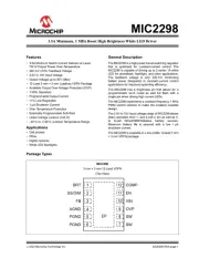
Microchip PIC32MZ1025DAR169 Manual
Microchip
Ikke kategoriseret
PIC32MZ1025DAR169
Læs gratis den danske manual til Microchip PIC32MZ1025DAR169 (122 sider) i kategorien Ikke kategoriseret. Denne vejledning er vurderet som hjælpsom af 14 personer og har en gennemsnitlig bedømmelse på 4.3 stjerner ud af 7.5 anmeldelser. Har du et spørgsmål om Microchip PIC32MZ1025DAR169, eller vil du spørge andre brugere om produktet?
Side 1/122

© 2015-2019 Microchip Technology Inc. DS60001344E-page 22-1
Section 22. 12-bit High-Speed Successive Approximation
Register (SAR) Analog-to-Digital Converter (ADC)
This section of the manual contains the following major topics:
22.1 Introduction .................................................................................................................. 22-2
22.2 Control Registers ......................................................................................................... 22-6
22.3 ADC Operation........................................................................................................... 22-61
22.4 ADC Module Configuration ........................................................................................ 22-65
22.5 Additional ADC Functions .......................................................................................... 22-85
22.6 Interrupts.................................................................................................................. 22-108
22.7 Operation During Power-Saving Modes .................................................................. 22-114
22.8 Effects of Reset........................................................................................................ 22-116
22.9 Transfer Function..................................................................................................... 22-116
22.10 ADC Sampling Requirements.................................................................................. 22-117
22.11 Connection Considerations...................................................................................... 22-117
22.12 Related Application Notes........................................................................................ 22-118
22.13 Revision History ....................................................................................................... 22-119

PIC32 Family Reference Manual
DS60001344E-page 22-2 © 2015-2019 Microchip Technology Inc.
22.1 INTRODUCTION
The PIC32 12-bit High-Speed Successive Approximation Register (SAR) Analog-to-Digital
Converter (ADC) includes the following features:
• 12-bit resolution
• Up to eight ADC modules with dedicated Sample and Hold (S&H) circuits (see Note 1)
• Two dedicated ADC modules can be combined in Turbo mode to provide double
conversion rate
• Single-ended and/or differential inputs
• Can operate during Sleep mode
• Supports touch sense applications
• Up to six digital comparators
• Up to six digital filters supporting two modes:
- Oversampling mode
- Averaging mode
• FIFO and DMA engine for dedicated ADC modules (see Note 2)
• Early interrupt generation resulting in faster processing of converted data
• Designed for motor control, power conversion, and general purpose applications
The dedicated ADC modules use a single input (or its alternate) and is intended for high-speed
and precise sampling of time-sensitive or transient inputs, whereas the shared ADC module
incorporates a multiplexer on the input to facilitate a larger group of inputs, with slower sampling,
and provides flexible automated scanning option through the input scan logic.
For each ADC module, the analog inputs are connected to the S&H capacitor. The clock,
sampling time, and output data resolution for each ADC module can be set independently. The
ADC module performs the conversion of the input analog signal based on the configurations set
in the registers. When conversion is complete, the final result is stored in the result buffer for the
specific analog input and is passed to the digital filter and digital comparator if configured to use
data from this particular sample.
A simplified block diagram of the ADC module is illustrated in Figure 22-1.
Note: This family reference manual section is meant to serve as a complement to device
data sheets. Depending on the device, this manual section may not apply to all
PIC32 devices.
Please refer to the note at the beginning of the “ADC” chapter in the current device
data sheet to check whether this document supports the device you are using.
Device data sheets and family reference manual sections are available for
download from the Microchip Worldwide Web site at: http://www.microchip.com
Note 1: Depending on the device, the 12-bit High-Speed SAR ADC has up to seven
dedicated ADC modules and one shared ADC module. Throughout this chapter,
the diagrams and code examples refer to a device with seven dedicated ADC
modules (ADC0-ADC6) and one shared ADC (ADC7). Please consult the “ADC”
chapter in the specific device data sheet to determine which ADC modules are
available for your device.
2: This feature is not available on all devices. Refer to the “ADC” chapter in the
specific device data sheet to determine availability.
3: Prior to enabling the ADC module, the user application must copy the ADC
calibration data (DEVADCx) from the Configuration memory into the ADC
Configuration registers (ADC0CFG-ADC7CFG). Refer to the “ADC” chapter in the
specific device data sheet for more information.

© 2015-2019 Microchip Technology Inc. DS60001344E-page 22-3
Section 22. 12-bit High-Speed SAR ADC
Figure 22-1: ADC Block Diagram
Note: The number of ADC modules, analog inputs, ANa, ANb, ANc, and ANd, and the FIFO and DMA features
are shown as an example. Refer to the “ADC” chapter in the specific device data sheet to determine the
actual ANx selections, ADC module availability, and the specific FIFO and DMA features.
ADC0
ADC7
AV
DD
AV
SS
V
REF
+ V
REF
-
VREFSEL<2:0>
V
REFH
V
REFL
ADCSEL<1:0>
CONCLKDIV<5:0>
T
CY
FRC PBCLK
T
Q
ADCDIV<6:0>
(ADCxTIME<22:16>)
ADCDIV<6:0>
(ADCCON2<6:0>)
T
AD0
-T
AD6
T
AD7
ADDATA0
…...
ADDATA63
(Dedicated
ADC)
(Dedicated
ADC)
FIFO
DMA
Digital Filter
Digital Comparator Interrupt/Event
Capacitive Voltage
Divider (CVD) Interrupt/Event
Triggers,
Turbo Channel,
Scan Control Logic
Trigger
Status and Control
Registers
ADC6
SH0ALT<1:0>
(ADCTRGMODE<17:16>)
ANx
V
REFL
0
1
DIFFx<1>
(ADCIMCONx<x>)
ANa
AN1
V
REFL
0
1
DIFF1<1>
(ADCIMCON1<3>)
SH6ALT<1:0>
(ADCTRGMODE<29:28>)
ANx
V
REFL
0
1
DIFFx<1>
(ADCIMCONx<x>)
AN49
IV
CTMU
IV
BAT
AN48
AN7
CVD
Capacitor
T
CLK
ANb
ANc
ANd
00
01
10
11
ANb
ANc
ANd
00
01
10
11
SYSTEMBUS
ANa
Interrupt
Data

PIC32 Family Reference Manual
DS60001344E-page 22-4 © 2015-2019 Microchip Technology Inc.
Figure 22-2: FIFO Block Diagram
FEN
(ADCFSTAT<31>
FIFO
(Depth Device Dependent)
ADCFIFO DATA<31:0>
ADCID<2:0>
ADCFSTAT<2:0> ADCx ID
ADCx ID Converted Data
ADC6
ADC6EN
(ADCFSTAT<30>)
ADC5
ADC5EN
(ADCFSTAT<29>)
ADC0
ADC0EN
(ADCFSTAT<24>)
If data
available in
FIFO
FRDY
ADCFSTAT<22>
FIEN
(ADCFSTAT<23>
Interrupt
FCNT<7:0>
ADCFSTAT<15:8>
(Number of data in FIFO)
Note: The number of ADC modules, analog inputs, ANa, ANb, ANc, and ANd, and the FIFO and DMA features
are shown as an example. Refer to the “ADC” chapter in the specific device data sheet to determine the
actual ANx selections, ADC module availability, and the specific FIFO and DMA features.

© 2015-2019 Microchip Technology Inc. DS60001344E-page 22-5
Section 22. 12-bit High-Speed SAR ADC
Figure 22-3: DMA Block Diagram
DMAGEN
(ADCDMASTAT<31>)
ADC6
DMAEN
(ADC6TIME<23>)
ADC5
ADC0
DMAEN
(ADC5TIME<23>)
DMAEN
(ADC0TIME<23>)
Buffer A (ADC0)
Buffer B (ADC0)
Buffer A (ADC1)
Buffer B (ADC1)
Buffer A (ADC6)
Buffer B (ADC6)
2
DMABL<2:0>
2
DMABL<2:0>
2
DMABL<2:0>
Buffer
Full?
RAF0
(ADCDMASTAT<0>)
RAFIEN0
(ADCDMASTAT<8>)
Interrupt
Buffer
Full?
RBF6
(ADCDMASTAT<22>)
RBFIEN6
(ADCDMASTAT<30>)
Interrupt
Data Count for Buffer-A
(ADC0)
Data Count for Buffer-B
(ADC0)
Data Count for Buffer-A
(ADC1)
Data Count for Buffer-B
(ADC1)
Data Count for Buffer-A
(ADC6)
Data Count for Buffer-B
(ADC6)
DMABADDR<31:0>
CNTBADDR<31:0>
CNTBADDR<31:0> + 1
CNTBADDR<31:0> + 2
CNTBADDR<31:0> + 3
Note: The number of ADC modules, analog inputs, ANa, ANb, ANc, and ANd, and the FIFO and DMA features
are shown as an example. Refer to the “ADC” chapter in the specific device data sheet to determine the
actual ANx selections, ADC module availability, and the specific FIFO and DMA features.

PIC32 Family Reference Manual
DS60001344E-page 22-6 © 2015-2019 Microchip Technology Inc.
22.2 CONTROL REGISTERS
The PIC32 12-bit High-Speed SAR ADC module has the following Special Function Registers
(SFRs):
•ADCCON1: ADC Control Register 1
This register controls the basic operation of all ADC modules, including behavior in Sleep
and Idle modes, and data formatting. This register also specifies the vector shift amounts for
the Interrupt Controller. Additional ADCCON1 functions include controlling the Turbo feature
of the ADC, the RAM buffer length in DMA mode, and Capacitive Voltage Division (CVD).
•ADCCON2: ADC Control Register 2
This register controls the reference selection for all ADC modules, the sample time for the
shared ADC module, interrupt enable for reference, early interrupt selection, and clock
division selection for the shared ADC.
•ADCCON3: ADC Control Register 3
This register enables ADC clock selection, enables/disables the digital feature for the
dedicated and shared ADC modules and controls the manual (software) sampling and
conversion.
•ADCTRGMODE: ADC Triggering Mode for Dedicated ADC Register
This register has selections for alternate analog inputs and includes trigger settings for the
dedicated ADC modules.
•ADCIMCON1: ADC Input Mode Control Register 1 through
ADCIMCON4: ADC Input Mode Control Register 4
These registers enable the user to select between single-ended and differential operation
as well as select between signed and unsigned data format.
•ADCGIRQEN1: ADC Global Interrupt Enable Register 1 and
ADCGIRQEN2: ADC Global Interrupt Enable Register 2
These registers specify which of the individual input conversion interrupts can generate the
global ADC interrupt.
•ADCCSS1: ADC Common Scan Select Register 1 and
ADCCSS2: ADC Common Scan Select Register 2
These registers specify the analog inputs to be scanned by the common scan trigger.
•ADCDSTAT1: ADC Data Ready Status Register 1 and
ADCDSTAT2: ADC Data Ready Status Register 2
These registers contain the interrupt status of the individual analog input conversions. Each
bit represents the data-ready status for its associated conversion result.
•ADCCMPENx: ADC Digital Comparator ‘x’ Enable Register (‘x’ = 1 through 6)
These registers select which analog input conversion results will be processed by the digital
comparator.
•ADCCMPx: ADC Digital Comparator ‘x’ Limit Value Register (‘x’ = 1 through 6)
These registers contain the high and low digital comparison values for use by the digital
comparator.
•ADCFLTRx: ADC Digital Filter ‘x’ Register (‘x’ = 1 through 6)
These registers provide control and status bits for the oversampling filter accumulator, and
also includes the 16-bit filter output data.
•ADCTRG1: ADC Trigger Source 1Register
This register controls the trigger source selection for AN0 through AN3 analog inputs.
•ADCTRG2: ADC Trigger Source 2 Register
This register controls the trigger source selection for AN4 through AN7 analog inputs.
•ADCTRG3: ADC Trigger Source 3 Register
This register controls the trigger source selection for AN8 through AN11 analog inputs.
•ADCTRG4: ADC Trigger Source 4 Register
This register controls the trigger source selection for AN12 through AN15 analog inputs.
•ADCTRG5: ADC Trigger Source 5 Register
This register controls the trigger source selection for AN16 through AN19 analog inputs.

© 2015-2019 Microchip Technology Inc. DS60001344E-page 22-13
Section 22. 12-bit High-Speed SAR ADC
bit 14 REFFLTIEN: Band Gap/V
REF
Voltage Fault Interrupt Enable bit
1 = Interrupt will be generated when the REFFLT bit is set
0 = No interrupt is generated when the REFFLT bit is set
bit 13 EOSIEN: End of Scan Interrupt Enable bit
1 = Interrupt will be generated when EOSRDY bit is set
0 = No interrupt is generated when the EOSRDY bit is set
bit 12 ADCEIOVR: Early Interrupt Request Override bit
1 = Early interrupt generation is overridden and interrupt generation is controlled by the ADCGIRQEN1
and ADCGIRQEN2 registers
0 = Early interrupt generation is not overridden and interrupt generation is controlled by the ADCEIEN1
and ADCEIEN2 registers
bit 11 ECRIEN: External Conversion Request Interface Enable bit
1 = Enables ADC conversion start from external module (such as PTG)
0 = External modules cannot start ADC conversion
bit 10-8 ADCEIS<2:0>: Shared ADC Early Interrupt Select bits
These bits select the number of clocks (T
AD
)
prior to the arrival of valid data that the associated interrupt
is generated.
111 = The data ready interrupt is generated 8 ADC clocks prior to end of conversion
110 = The data ready interrupt is generated 7 ADC clocks prior to end of conversion
•
•
•
001 = The data ready interrupt is generated 2 ADC module clocks prior to end of conversion
000 = The data ready interrupt is generated 1 ADC module clock prior to end of conversion
Note: All options are available when the selected resolution, set by the SELRES<1:0> bits
(ADCCON1<22:21>), is 12-bit or 10-bit. For a selected resolution of 8-bit, options from ‘000’ to
‘101’ are valid. For a selected resolution of 6-bit, options from ‘000’ to ‘011’ are valid.
bit 7 Unimplemented: Read as ‘0’
bit 6-0 ADCDIV<6:0>: Shared ADC Clock Divider bits
1111111 = 254 * T
Q
= T
AD
•
•
•
0000011 = 6 * T
Q
= T
AD
0000010 = 4 * T
Q
= T
AD
0000001 = 2 * T
Q
= T
AD
0000000 = Reserved
The ADCDIV<6:0> bits divide the ADC control clock (T
Q
) to generate the clock for the Shared ADC (T
AD
).
Register 22-2: ADCCON2: ADC Control Register 2 (Continued)

PIC32 Family Reference Manual
DS60001344E-page 22-14 © 2015-2019 Microchip Technology Inc.
Register 22-3: ADCCON3: ADC Control Register 3
Bit
Range
Bit
31/23/15/7
Bit
30/22/14/6
Bit
29/21/13/5
Bit
28/20/12/4
Bit
27/19/11/3
Bit
26/18/10/2
Bit
25/17/9/1
Bit
24/16/8/0
31:24
R/W-0 R/W-0 R/W-0 R/W-0 R/W-0 R/W-0 R/W-0 R/W-0
ADCSEL<1:0> CONCLKDIV<5:0>
23:16
R/W-0 R/W-0 R/W-0 R/W-0 R/W-0 R/W-0 R/W-0 R/W-0
DIGEN7
(5)
DIGEN6
(5)
DIGEN5
(5)
DIGEN4
(5)
DIGEN3
(5)
DIGEN2
(5)
DIGEN1
(5)
DIGEN0
(5)
15:8
R/W-0 R/W-0 R/W-0 R/W-0 R/W-0 R-0, HS, HC R/W-0 R-0, HS, HC
VREFSEL<2:0> TRGSUSP UPDIEN UPDRDY SAMP
(1,2,3,4)
RQCNVRT
7:0
R/W-0 R-0, HS, HC R/W-0 R/W-0 R/W-0 R/W-0 R/W-0 R/W-0
GLSWTRG GSWTRG ADINSEL<5:0>
(5)
Legend: HC = Hardware Set HS = Hardware Cleared
R = Readable bit W = Writable bit U = Unimplemented bit, read as ‘0’
-n = Value at POR ‘1’ = Bit is set ‘0’ = Bit is cleared x = Bit is unknown
bit 31-30 ADCSEL<1:0>: Analog-to-Digital Clock Source (T
CLK
) bits
Refer to the “12-bit High-Speed Successive Approximation Register (SAR)” chapter in the specific
device data sheet for the ADC Clock source selections.
bit 29-24 CONCLKDIV<5:0>: Analog-to-Digital Control Clock (T
Q
) Divider bits
111111 = 126 * T
CLK
= T
Q
•
•
•
000011 = 6 * T
CLK
= T
Q
000010 = 4 * T
CLK
= T
Q
000001 = 2 * T
CLK
= T
Q
000000 = T
CLK
= T
Q
bit 23 DIGEN7: ADC7 Digital Enable bit
(5)
1 = ADC7 is digital enabled
0 = ADC7 is digital disabled
bit 22 DIGEN6: ADC6 Digital Enable bit
(5)
1 = ADC6 is digital enabled
0 = ADC6 is digital disabled
bit 21 DIGEN5: ADC5 Digital Enable bit
(5)
1 = ADC5 is digital enabled
0 = ADC5 is digital disabled
bit 20 DIGEN4: ADC4 Digital Enable bit
(5)
1 = ADC4 is digital enabled
0 = ADC4 is digital disabled
Note 1: The SAMP bit has the highest priority and setting this bit will keep the S&H circuit in Sample mode until the
bit is cleared. Also, usage of the SAMP bit will cause settings of the SAMC<9:0> bits (ADCCON2<25:16>)
to be ignored.
2: The SAMP bit only connects Class 2 and Class 3 analog inputs to the shared ADC. All Class 1 analog
inputs are not affected by the SAMP bit.
3: The SAMP bit is not a self-clearing bit and it is the responsibility of application software to first clear this bit
and only after setting the RQCNVRT bit to start the analog-to-digital conversion.
4: Normally, when the SAMP and RQCNVRT bits are used by software routines, all TRGSRCx<4:0> bits and
STRGSRC<4:0> bits should be set to ‘00000’ to disable all external hardware triggers and prevent them
from interfering with the software-controlled sampling command signal SAMP and with the
software-controlled trigger RQCNVRT.
5: Depending on the device, the function will vary. Refer to the “ADC” chapter in the specific device data
sheet to determine the function that is available for your device.

© 2015-2019 Microchip Technology Inc. DS60001344E-page 22-17
Section 22. 12-bit High-Speed SAR ADC
Register 22-4: ADCTRGMODE: ADC Triggering Mode for Dedicated ADC Register
Bit
Range
Bit
31/23/15/7
Bit
30/22/14/6
Bit
29/21/13/5
Bit
28/20/12/4
Bit
27/19/11/3
Bit
26/18/10/2
Bit
25/17/9/1
Bit
24/16/8/0
31:24
U-0 U-0 R/W-0 R/W-0 R/W-0 R/W-0 R/W-0 R/W-0
— — SH6ALT<1:0> SH5ALT<1:0> SH4ALT<1:0>
23:16
R/W-0 R/W-0 R/W-0 R/W-0 R/W-0 R/W-0 R/W-0 R/W-0
SH3ALT<1:0> SH2ALT<1:0> SH1ALT<1:0> SH0ALT<1:0>
15:8
U-0 R/W-0 R/W-0 R/W-0 R/W-0 R/W-0 R/W-0 R/W-0
— STRGEN6 STRGEN5 STRGEN4 STRGEN3 STRGEN2 STRGEN1 STRGEN0
7:0
U-0 R/W-0 R/W-0 R/W-0 R/W-0 R/W-0 R/W-0 R/W-0
— SSAMPEN6 SSAMPEN5 SSAMPEN4 SSAMPEN3 SSAMPEN2 SSAMPEN1 SSAMPEN0
Legend:
R = Readable bit W = Writable bit U = Unimplemented bit, read as ‘0’
-n = Value at POR ‘1’ = Bit is set ‘0’ = Bit is cleared x = Bit is unknown
bit 31-30 Unimplemented: Read as ‘ ’
bit 29-28 SH6ALT<1:0>: ADC6 Analog Input Select bit
11 01 - = Refer to the “ADC” chapter in the specific device data sheet for the available selections
00 = AN6
bit 27-26 SH5ALT<1:0>: ADC5 Analog Input Select bit
11 01 - = Refer to the “ADC” chapter in the specific device data sheet for the available selections
00 = AN5
bit 25-24 SH4ALT<1:0>: ADC4 Analog Input Select bit
11 01 - = Refer to the “ADC” chapter in the specific device data sheet for the available selections
00 = AN4
bit 23-22 SH3ALT<1:0>: ADC3 Analog Input Select bit
11 01 - = Refer to the “ADC” chapter in the specific device data sheet for the available selections
00 = AN3
bit 21-20 SH2ALT<1:0>: ADC2 Analog Input Select bit
11 01 - = Refer to the “ADC” chapter in the specific device data sheet for the available selections
00 = AN2
bit 19-18 SH1ALT<1:0>: ADC1 Analog Input Select bit
11 01 - = Refer to the “ADC” chapter in the specific device data sheet for the available selections
00 = AN1
bit 17-16 SH0ALT<1:0>: ADC0 Analog Input Select bit
11 01 - = Refer to the “ADC” chapter in the specific device data sheet for the available selections
00 = AN0
bit 15 Unimplemented: Read as ‘ ’
bit 14 STRGEN6: ADC6 Presynchronized Triggers bit
1 = ADC6 uses presynchronized triggers
0 = ADC6 does not use presynchronized triggers
bit 13 STRGEN5: ADC5 Presynchronized Triggers bit
1 = ADC5 uses presynchronized triggers
0 = ADC5 does not use presynchronized triggers
bit 12 STRGEN4: ADC4 Presynchronized Triggers bit
1 = ADC4 uses presynchronized triggers
0 = ADC4 does not use presynchronized triggers
bit 11 STRGEN3: ADC3 Presynchronized Triggers bit
1 = ADC3 uses presynchronized triggers
0 = ADC3 does not use presynchronized triggers

© 2015-2019 Microchip Technology Inc. DS60001344E-page 22-19
Section 22. 12-bit High-Speed SAR ADC
Register 22-5: ADCIMCON1: ADC Input Mode Control Register 1
Bit Range Bit
31/23/15/7
Bit
30/22/14/6
Bit
29/21/13/5
Bit
28/20/12/4
Bit
27/19/11/3
Bit
26/18/10/2
Bit
25/17/9/1
Bit
24/16/8/0
31:24
R/W-0 R/W-0 R/W-0 R/W-0 R/W-0 R/W-0 R/W-0 R/W-0
DIFF15 SIGN15 DIFF14 SIGN14 DIFF13 SIGN13 DIFF12 SIGN12
23:16
R/W-0 R/W-0 R/W-0 R/W-0 R/W-0 R/W-0 R/W-0 R/W-0
DIFF11 SIGN11 DIFF10 SIGN10 DIFF9 SIGN9 DIFF8 SIGN8
15:8
R/W-0 R/W-0 R/W-0 R/W-0 R/W-0 R/W-0 R/W-0 R/W-0
DIFF7 SIGN7 DIFF6 SIGN6 DIFF5 SIGN5 DIFF4 SIGN4
7:0
R/W-0 R/W-0 R/W-0 R/W-0 R/W-0 R/W-0 R/W-0 R/W-0
DIFF3 SIGN3 DIFF2 SIGN2 DIFF1 SIGN1 DIFF0 SIGN0
Legend:
R = Readable bit W = Writable bit U = Unimplemented bit, read as ‘0’
-n = Value at POR ‘1’ = Bit is set ‘0’ = Bit is cleared x = Bit is unknown
bit 31 DIFF15: AN15 Mode bit
1 = AN15 is using Differential mode
0 = AN15 is using Single-ended mode
bit 30 SIGN:15 AN15 Signed Data Mode bit
1 = AN15 is using Signed Data mode
0 = AN15 is using Unsigned Data mode
bit 29 DIFF14: AN14 Mode bit
1 = AN14 is using Differential mode
0 = AN14 is using Single-ended mode
bit 28 SIGN14: AN14 Signed Data Mode bit
1 = AN14 is using Signed Data mode
0 = AN14 is using Unsigned Data mode
bit 27 DIFF13: AN13 Mode bit
1 = AN13 is using Differential mode
0 = AN13 is using Single-ended mode
bit 26 SIGN13: AN13 Signed Data Mode bit
1 = AN13 is using Signed Data mode
0 = AN13 is using Unsigned Data mode
bit 25 DIFF12: AN12 Mode bit
1 = AN12 is using Differential mode
0 = AN12 is using Single-ended mode
bit 24 SIGN12: AN12 Signed Data Mode bit
1 = AN12 is using Signed Data mode
0 = AN12 is using Unsigned Data mode
bit 23 DIFF11: AN11 Mode bit
1 = AN11 is using Differential mode
0 = AN11 is using Single-ended mode
bit 22 SIGN11: AN11 Signed Data Mode bit
1 = AN11 is using Signed Data mode
0 = AN11 is using Unsigned Data mode
bit 21 DIFF10: AN10 Mode bit
1 = AN10 is using Differential mode
0 = AN10 is using Single-ended mode
Produkt Specifikationer
Mærke: | Microchip |
Kategori: | Ikke kategoriseret |
Model: | PIC32MZ1025DAR169 |
Har du brug for hjælp?
Hvis du har brug for hjælp til Microchip PIC32MZ1025DAR169 stil et spørgsmål nedenfor, og andre brugere vil svare dig
Ikke kategoriseret Microchip Manualer
17 Juni 2025
17 Juni 2025
17 Juni 2025
17 Juni 2025
17 Juni 2025
17 Juni 2025
17 Juni 2025
18 Februar 2025
18 Februar 2025
18 Februar 2025
Ikke kategoriseret Manualer
- Mosconi
- Sencor
- Portech
- Ursus Trotter
- Solid
- OKI
- Cayin
- Dash
- Nearity
- Texas Instruments
- Revox
- Bartscher
- Nexcom
- Shape
- Kyocera
Nyeste Ikke kategoriseret Manualer
17 Juni 2025
17 Juni 2025
17 Juni 2025
17 Juni 2025
17 Juni 2025
17 Juni 2025
17 Juni 2025
17 Juni 2025
17 Juni 2025
17 Juni 2025