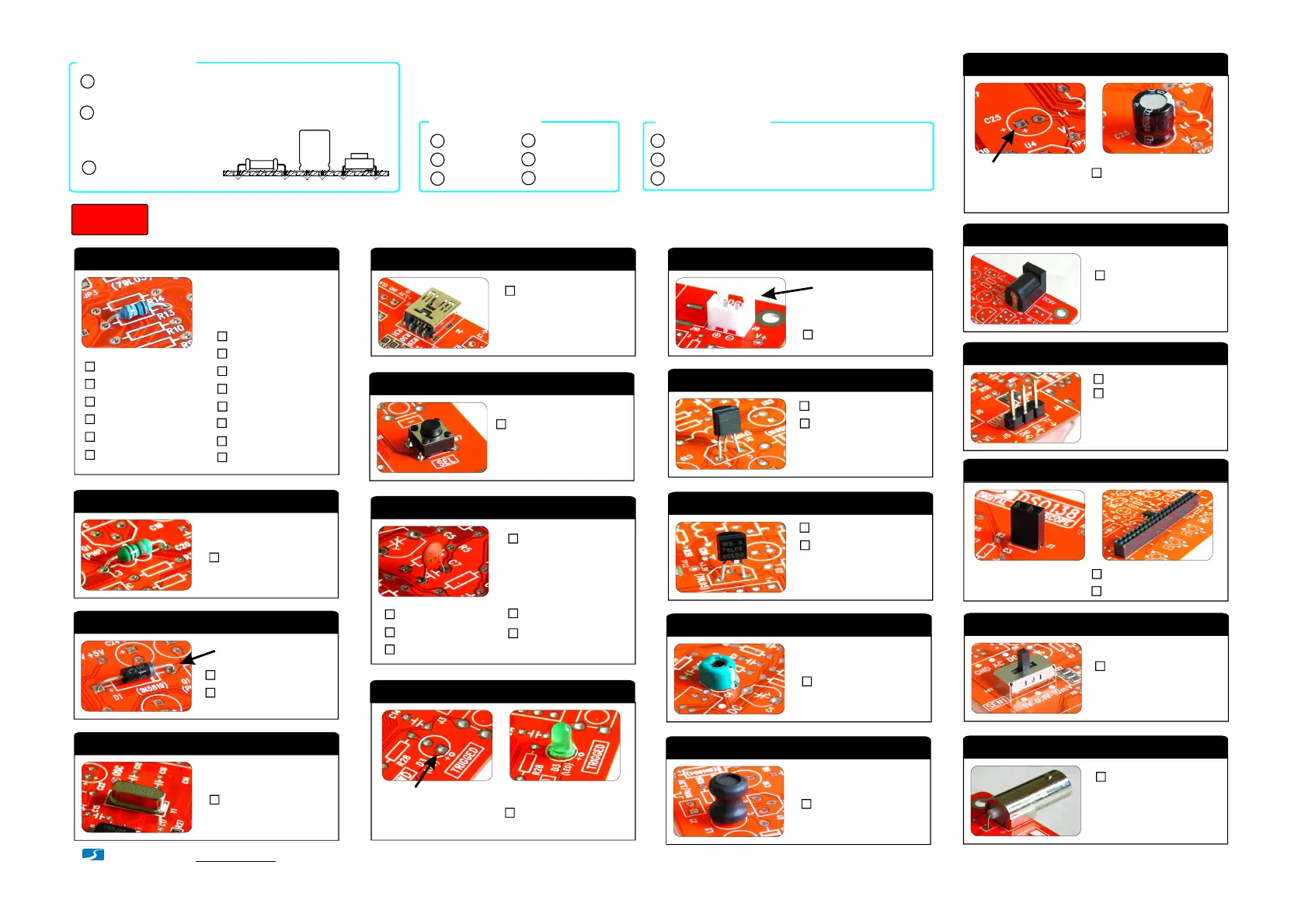
Joy-It DSO-138 Manual


Læs gratis den danske manual til Joy-It DSO-138 (4 sider) i kategorien Ikke kategoriseret. Denne vejledning er vurderet som hjælpsom af 30 personer og har en gennemsnitlig bedømmelse på 3.7 stjerner ud af 15.5 anmeldelser. Har du et spørgsmål om Joy-It DSO-138, eller vil du spørge andre brugere om produktet?

Side 1/4
Ir (on 20W)1
Solder wire
Multimeter
Sc e err w d vri
User Manual
Rev. 05
D DSO 138 Oscilloscope IY Kit
2
3
4
Flush cutter5
Too yo nls u eed
Tweezers
6
Assemb a a an a ed)ly M in Bo rd d d LCD boar ( rfo o oll w the der s nu bm er
Step 1
- www. ye .comj tech -
JY LE Tech td.
1 o. Resi ts rs
Alway ors r mete resist
v be or oldalues f e s ering
Note:
R R R1, 14, 16 1 0K0 Ω
R2 1 8M. Ω
:
:
R3 2 0K0 Ω:
R4 2MΩ:
R5 20KΩ:
R6 300Ω:
R R7, 36 180Ω
R R R8, 12, 13
120Ω
:
:
R R R9, 15, 26
1KΩ
:
R10
3KΩ
:
R38
1 5K. Ω
:
R R28, 40
470Ω
:
R R37, 39
10KΩ
:
L L1, 3,L4 100 Hμ
2 ho. HF-C kes
:
D1 1N5819
3 od. Di es
:
D2 1N4004
:
(o 4 07)r 1N 0
Y1 8MHz
4. Crystal
:
J4 USB mini - B
5 ocke. USB S t *
:
6 6 X X 5mm
6. Ta esc cht Swit
:
S SW4, W5,
S 6 7,W , SW
SW8
7 o. Ce ar mic Cap ca it rs
0.1 F
μ
:
3 03 pF:
3pF:
C1 9, C ,
C10 1,, C1
C14 15,, C
C16 17,, C
C18 20,, C
C23
1pF:
C C7, 8
120 pF
:
C C12, 13
2 pF2
:
C2
C3
C5
D3
8. LED
:
φ3 grmm, een
So ol itide por s v pe le
(t l l tohe onger ead)
th quae s re pad
J9 2 Pin
9 de o o. Pin hea r (f r p wer)
:
Fa ece e th op ning
outward
8550
10. Tr rsan osist
:
Q1
9014
:
Q2
Cathode
79 05L
11. Regu ol ta rs
:
U4
78L05
:
U5
C C64, 5 - 30pF
1 o2. Cap ca it r t ir mmers
:
L2 1 0 5AmH/ .
13 n uc or. Power i d t
:
1 o y o4. Electr l ti itc c capa rs
:
100μ/ 1 6VF
So ol itide por s v pe le
(t l l tohe onger ead)
th quae s re pad
C19 21,, C
C22 24,, C
C25 26, C
DC005
1 o or5. P wer con ecn t
:
J10
1 n h6. Pi - e eader (mal ) *
1 3 X pin
:
J5
1 4 X pin
:
J6
17 n h. Pi - e eader (f male)
:
1 X 2 pin
J7 J8,
:
2 X 0 2 pin
J3
S SW1, W2,
SW3
2 3TP
18. Slide switches
:
J1 BNC
1 ne9. BNC con ctor
:
Pu ou ou ht leads thr gh m nting o o h dles fr m t e si e with
pa linert out . En us e c e e eo onmp nt v nly touch PCB.
1
Sold ot d h ul ullye ar leads t the her si e. Solder s o d f
f rill a c end ov r solde ing pads.
Av b d boid ri ges et enwe
n gh p dei b neri g a s.
Cu u dst nused lea
flu uttsh with c er.
2
3
So d nl eri g Hints
Ch v q gec ak p rt al eu s & u nta ities a ai an pst rt list1
Al i lde ingwa ete eys m r r s s st lo vr a ue es b f ro e o r
Und n p po n nse arst d all art l iarit e as d o n orie tati
2
3
Be afore you st rt
Page 1
Packa e ar ag s e simil r.
Do x not mi up!
Atten n!tio
Packa e ar ag s e simil r.
Do x not mi up!
Atten n!tio
Th h e n ee t ick r pi s n ed
t he u e geto at p long r to
g o old ult.o d s erin reg s
Note:
R11 150Ω
:
Th aes pin hee - der ares
o al.p ntio
Note:
App b dlica le mo els: 13803K, 1 4K3 08
I r f r rn pstal all l SMD a ts be o e p o ngceedi
t te io S p y u h1 if o pu rc ased k t 13 048 K.
Important !!!
Th o eis c nn ctor is
op ntio al.
Note:
Ap wp blica le firm a 1 1 are: 1 3- 3801 06 o- 0 r l ter
1
C. Ver fi y
Co p hnnect o ower .supply again Y u s ould see LCD
li t ill is lagh s up and osc o dscope panel p yed.
2Pr riess va o o v vu bus tt n os and m e switches to erify
their func oti ns.
1 g ) Make a small rin with a
. lead cut-off
20 na. Test sig l ring
2 0 X 2 pin
2 o2. LCD B ard
:
J1
1 2 X pin
:
J J32,
2 ) r So del the ring o t the two
holes of J2 (as shown in
. the p o oh t )
21. JP3
S Phort J 3 h wit solder Note: In hstal t tl o e side
o itppos e o D t LC p na el.
Test and Use
Step 2
3 y n y d ) V C r A 9 D powe su pp l (> 200mA c acap ity) is r requi ed to ru th oe sc pe. Po u pwer s p l is not i lnc ude in the kit.
1
A. Check voltages
2
3
Ap 1 9p 9 poly V wer to J 0 (or J ).
2Ch o 2 o 3eck v ltage at TP2 . It sh u bld e around + .3V.
3I rf r v golta e at TP22 is good d o necisc n t powe . Sho t JP4
with solder .permanently 1
B. Attach LCD board
Pl i t tug d LCD boar n o h de e femal hea er ans , , J3 J7 d J8
on t ihe ma n board.
1
A. Use
Att tac cliph p bro e s o J1.
2To h y g guch t e red clip with ou nr fi er. Do you see si nal
fr fi r?o yom ur nge
1
- www. y . omj e ect h c -JYE Tech Ltd.
Tro oou hbles ting
Is vo glta e at V+
go d?o Ch poweck er
supply
I rrs R36 v oalue c ect
a e en dd sol r d g od?o
D y b uo o gu e at o t 3V
b p 1e etw en 1 J in 6 &
1 o b d?8 n LCD oar
Fix R36
LCD Dark
No
No
Yes
Yes
(No b kac light)
No
Yes
Ch 3 ndeck R 6 a
po gwe ar ain
C CDheck L
board
P Sress W8. Does LED b nli k? C C Che 1ck Y , 12, 13
Che n onck LED i st l ia l ta
Che 3. vock + 3V ltage
Che o de ock 3 J s l ring f r
po b op n o hssi le e s r s orts
N Dio splay
Yes
No
Che o de ock 1 J s l ring n LCD
bo o po opeard f r ssi lb e ns
o ho odr s rts e (us Test M e)
2
8 6. 0V
9 9V.3
8 4V.3
3.3V
-1 3. 9V
2 6V.1
0 1V.8
6 3V.40 9V.1
5 2V.03.3V4 9V.9-5 0V.
-8 0. 8V
-8 1V.1
1 6V0V .6
*
*
**
*
*
*
**
**
Vo gelta
Re e esf re cn
(Inp o gut V lta e)
* h vo g npu vo p nd n h v u: T ese lta e as re i t lta eg de e e t. T e al es
s s show wn e ere m a ured w wh npu o gen i t v lta e a 9 39. V.
** vo g u h: e Thes lta e a es re m as red w en h CPL switc (SW1)
is set to GND po on.si it
NOTES:
Pl t tac a ee th nee g tiv pe n o of v l -me er
he ag e enre t lo o d vo t e measur m ts.
Fi i lon shed ok
Sh Port J 4 if it has not been
do ve.n oe e ab. S e p 2 Ste
C Bheck U2 , U2C and
rel t ta e ard p s around
t t m li ihese wo a p f ers
No
Set CPL switch to GND
a eand m sure V1 d an V2.
Ar rre they co ect?
Ch 1eck R 2 d an C8
Visi t ilt m f ro u fo dr e a ed
t ti iroub oolesh n ug g de
A Vre the v ual es of A + and
AV- c eorr ct?
No Trace
Yes
No
Yes
Th o h ph o n oe v l i ttages n e oto are f r r fere e ce nly.
Th o o y u o ou d ne v ltages n o r b a crd ld be iffere t.
Bu u b h v u o n.t they sho ld e close to t e al es sh w
NOTE 1:
www.j t m fye e cch. o / orum
Tech S pu port:
Trigger LED b nkli i t iceng w
i ti ind b oicates o ng-up s g od.o
Page 2
Test Mode
Wha o ot i it s and h w it w rks
Te e en a as M st od ue is d o d e t fin out p bossi l op s (for l il port p ns) nd shorts
(f - ) r fo p n 1r i s 0 5 d PB - 1 an PC 3 15 . n Whe e ent ed it irst d checks PB an PC
pi t i ln pe ps h wit s c ai l a t t ierns o f nd out poss b ho ounle s rt I fs. f d LED wi l be
f r ras e et . b k glin in Oth rwise, it gen a a ete 3.3V nd 0V alt n ve pati ly h at e ca ort
p n yc o d h gna bei s , , d n (PA PB PC an PD) i c le f abo cout 4 se n s. T ese si ls n ca
u o ose ch cd o t e k f r pens.
How to use
H wo dold n 4 d o SW an press RESET t e enter T st Mode.
I f r rf u e yo se LED as a et g b klin in th t m an hes t e e ar sho ts n o PB or PC p ni s.
Yo h ou d o d nee t fin out t e sh rt t.s f ri s
I l l l t t l tf u e yo se LED s o bwly i ink ng e us a vo t-me er o k h n c ech eac pi re a ed
c a Who hnne oncti s t t e d . ar su pes c et open e e a cn u yo dont s e volt ge hange
a c e co et a spot whi h d is suppose b ing n p hnec et d o a t o prt in t re y e ma b
op be h po h po p n.en tween t e s t d an t e rt i
1.
2.
3.
PIN 1
Ma ank ue s re U1 d g LED wo kr in
( ry b nou see LED li k ps twice at essing
RE ES T) b oef re u osing T est M de.
NOTE 3:
L b n nED will e b nk nli i g co sta tl iy f MCU
(U1 n d va n o) can ot etect lid LCD co tr ller.
Che n de g.ck LCD pi -hea r sold neri
NOTE 2:
1 d 6 ) , ,JP1 JP2 JP5 n, a JP at b oott m s side hould be kept op oen f r no nn nrmal ru i g mode.
2 d n ) B r The US c conne to do not h u oave f ncti n. It was p or v di e for f ru ut e or u oser w use.
Notes:


Produkt Specifikationer

Mærke: Joy-It
Kategori: Ikke kategoriseret
Model: DSO-138

Har du brug for hjælp?

Hvis du har brug for hjælp til Joy-It DSO-138 stil et spørgsmål nedenfor, og andre brugere vil svare dig