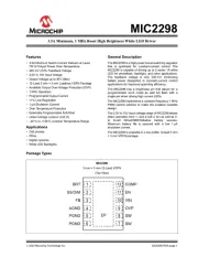
Microchip PIC24HJ128GP202 Manual

Microchip Ikke kategoriseret PIC24HJ128GP202

Læs gratis den danske manual til Microchip PIC24HJ128GP202 (72 sider) i kategorien Ikke kategoriseret. Denne vejledning er vurderet som hjælpsom af 11 personer og har en gennemsnitlig bedømmelse på 4.4 stjerner ud af 6 anmeldelser. Har du et spørgsmål om Microchip PIC24HJ128GP202, eller vil du spørge andre brugere om produktet?

Side 1/72
© 2007 Microchip Technology Inc. DS70225B-page 16-1
ADC
16
Section 16. Analog-to-Digital Converter (ADC)
HIGHLIGHTS
This section of the manual contains the following major topics:
16.1 Introduction .................................................................................................................. 16-2
16.2 Control Registers ......................................................................................................... 16-4
16.3 A/D Terminology and Conversion Sequence ............................................................. 16-14
16.4 ADC Module Configuration ........................................................................................ 16-16
16.5 Selecting the Voltage Reference Source ................................................................... 16-16
16.6 Selecting the A/D Conversion Clock .......................................................................... 16-17
16.7 Selecting Analog Inputs for Sampling ........................................................................ 16-18
16.8 Enabling the Module .................................................................................................. 16-20
16.9 Specifying Sample/Conversion Control...................................................................... 16-20
16.10 How to Start Sampling ............................................................................................... 16-21
16.11 How to Stop Sampling and Start Conversions ........................................................... 16-22
16.12 Controlling Sample/Conversion Operation................................................................. 16-32
16.13 Specifying Conversion Results Buffering ................................................................... 16-33
16.14 Conversion Sequence Examples............................................................................... 16-37
16.15 A/D Sampling Requirements...................................................................................... 16-55
16.16 Reading the ADC Result Buffer ................................................................................. 16-56
16.17 Transfer Function (10-bit Mode)................................................................................. 16-58
16.18 Transfer Function (12-bit Mode)................................................................................. 16-59
16.19 ADC Accuracy/Error................................................................................................... 16-60
16.20 Connection Considerations........................................................................................16-60
16.21 Code Examples.......................................................................................................... 16-60
16.22 Operation During Sleep and Idle Modes.................................................................... 16-67
16.23 Effects of a Reset....................................................................................................... 16-68
16.24 Special Function Registers Associated with the ADC................................................ 16-68
16.25 Design Tips ................................................................................................................ 16-70
16.26 Related Application Notes.......................................................................................... 16-71
16.27 Revision History ......................................................................................................... 16-72
© 2007 Microchip Technology Inc. DS70225B-page 16-2
Section 16. Analog-to-Digital Converter (ADC)
ADC
16
16.1 INTRODUCTION
The PIC24H family devices have up to 32 A/D input channels. These devices also have up to two
ADC modules (ADCx, where x = 1 or 2), each with its own set of Special Function Registers
(SFRs).
The 10-bit or 12-bit Operation Mode (AD12B) bit in the ADCx Control 1(ADxCON1) register
allows each of the ADC modules to be configured by the user application as either a 10-bit,
4 Sample/Hold (S/H) ADC (default configuration) or a 12-bit, 1 Sample/Hold ADC.
The 10-bit ADC configuration (AD12B = ) has the following key features:0
Successive Approximation (SAR) conversion
Conversion speeds of up to 1.1 Msps
Up to 32 analog input pins
External voltage reference input pins
Simultaneous sampling of up to four analog input pins
Automatic Channel Scan mode
Selectable conversion trigger source
Selectable Buffer Fill modes
DMA support, including Peripheral Indirect Addressing
Four result alignment options (signed/unsigned, fractional/integer)
Operation during CPU Sleep and Idle modes
Depending on the particular device pinout, the ADC can have up to 32 analog input pins,
designated AN0 through AN31. In addition, there are two analog input pins for external voltage
reference connections. These voltage reference inputs can be shared with other analog input
pins. The actual number of analog input pins and external voltage reference input configuration
will depend on the specific device. For further details, refer to the device data sheet.
The analog inputs are multiplexed to four Sample/Hold amplifiers, designated CH0-CH3. One,
two, or four of the Sample/Hold amplifiers can be enabled for acquiring input data. The analog
input multiplexers can be switched between two sets of analog inputs during conversions.
Unipolar differential conversions are possible on all channels using certain input pins (refer to
Figure 16-1).
An Analog Input Scan mode can be enabled for the CH0 Sample/Hold Amplifier. A Control
register specifies which analog input channels are included in the scanning sequence.
The ADC is connected to a single-word result buffer; however, multiple conversion results can
be stored in a DMA RAM buffer with no CPU overhead. Each conversion result is converted to
one of four 16-bit output formats when it is read from the buffer.
The 12-bit ADC configuration (AD12B = 1) supports all the features described, except:
In the 12-bit configuration, conversion speeds of up to 500 ksps are supported
There is only one Sample/Hold amplifier in the 12-bit configuration, so simultaneous
sampling of multiple channels is not supported
Note: The ADC module needs to be disabled before the AD12B bit is modified.


Produkt Specifikationer

Mærke: Microchip
Kategori: Ikke kategoriseret
Model: PIC24HJ128GP202

Har du brug for hjælp?

Hvis du har brug for hjælp til Microchip PIC24HJ128GP202 stil et spørgsmål nedenfor, og andre brugere vil svare dig