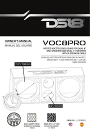
Microchip PIC24EP512GU814 Manual
Microchip
Ikke kategoriseret
PIC24EP512GU814
Læs gratis den danske manual til Microchip PIC24EP512GU814 (96 sider) i kategorien Ikke kategoriseret. Denne vejledning er vurderet som hjælpsom af 23 personer og har en gennemsnitlig bedømmelse på 4.3 stjerner ud af 12 anmeldelser. Har du et spørgsmål om Microchip PIC24EP512GU814, eller vil du spørge andre brugere om produktet?
Side 1/96

© 2010-2013 Microchip Technology Inc. DS70621C-page 16-1
Analog-to-Digital
Converter (ADC)
16
Section 16. Analog-to-Digital Converter (ADC)
HIGHLIGHTS
This section of the manual contains the following major topics:
16.1 Introduction .................................................................................................................. 16-2
16.2 Control Registers .........................................................................................................16-6
16.3 Overview of Sample and Conversion Sequence ....................................................... 16-17
16.4 ADC Configuration ..................................................................................................... 16-28
16.5 ADC Interrupt Generation ..........................................................................................16-35
16.6 Analog Input Selection for Conversion....................................................................... 16-37
16.7 Specifying Conversion Results Buffering for Devices with DMA and with ADC DMA Enable
Bit (ADDMAEN) Set ................................................................................................... 16-52
16.8 ADC Configuration Example ...................................................................................... 16-56
16.9 ADC Configuration for 1.1 Msps ................................................................................ 16-57
16.10 Sample and Conversion Sequence Examples for Devices without DMA and for Devices
with DMA but with ADC DMA Enable Bit (ADDMAEN) Clear .................................... 16-59
16.11 Sample and Conversion Sequence Examples for Devices with DMA and with ADDMAEN
Bit Set ........................................................................................................................ 16-71
16.12 Configuration Examples for Devices with Internal Op Amps ..................................... 16-81
16.13 Analog-to-Digital Sampling Requirements ................................................................. 16-84
16.14 Reading the ADC Result Buffer ................................................................................. 16-85
16.15 Transfer Functions ..................................................................................................... 16-87
16.16 ADC Accuracy/Error................................................................................................... 16-89
16.17 Connection Considerations........................................................................................ 16-89
16.18 Operation During Sleep and Idle Modes.................................................................... 16-89
16.19 Effects of a Reset....................................................................................................... 16-90
16.20 Design Tips ................................................................................................................ 16-91
16.21 Related Application Notes.......................................................................................... 16-92
16.22 Revision History ......................................................................................................... 16-93

dsPIC33E/PIC24E Family Reference Manual
DS70621C-page 16-2 © 2010-2013 Microchip Technology Inc.
16.1 INTRODUCTION
This document describes the features and associated operational modes of the Successive
Approximation (SAR) Analog-to-Digital Converter (ADC) modules available on the
dsPIC33E/PIC24E families of devices.
This ADC module can be configured by the user application to function as a 10-bit, 4-channel
ADC or a 12-bit, single channel ADC.
On devices with Direct Memory Access (DMA), this ADC module can be configured to use DMA
or use a dedicated, 16-word memory mapped buffer instead of DMA.
An ADC module block diagram for devices without op amps is provided in Figure 16-1. The ADC
module block diagram for devices with op amps is provided in Figure 16-2.
The following key features are common to all dsPIC33E/PIC24E devices:
• SAR conversion
• Up to 1.1 Msps conversion speed in 10-bit mode
• Up to 500 ksps conversion speed in 12-bit mode
• Up to 32 analog input pins
• External voltage reference input pins
• Four unipolar, differential Sample-and-Hold (S&H) amplifiers
• Simultaneous sampling of up to four analog input pins
• Automatic Channel Scanning mode
• Selectable conversion trigger source
• Up to 16-word conversion result buffer
• Operation during CPU Sleep and Idle modes
Additional features are available on select dsPIC33E/PIC24E devices:
• Connections for up to three internal op amps (not available on all devices)
• Connections to the Charge Time Measurement Unit (CTMU) and temperature
measurement diode (not available on all devices)
• Channel selection and triggering can be controlled by the Peripheral Trigger Generator
(PTG) (not available on all devices)
• Selectable Buffer Fill modes (not available on all devices)
• DMA support, including Peripheral Indirect Addressing (PIA) (not available on all devices)
Depending on the device variant, the ADC module may have up to 49 analog input pins, designated
AN0-AN48, and four op amp outputs, designated OA1-OA3 and OA5. These analog inputs and
op amp outputs are connected by multiplexers to four S&H amplifiers, designated CH0-CH3. The
analog input multiplexers have two sets of control bits, designated as MUXA (CHySA/CHyNA) and
MUXB (CHySB/CHyNB). These control bits select a particular analog input for conversion. The
MUXA and MUXB control bits can alternatively select the analog input for conversion. Unipolar
differential conversions are possible on all channels using certain input pins.
Note: This family reference manual section is meant to serve as a complement to device
data sheets. Depending on the device variant, this manual section may not apply to
all dsPIC33E/PIC24E devices.
Please consult the note at the beginning of the “Analog-to-Digital Converter
(ADC)” chapter in the current device data sheet to check whether this document
supports the device you are using.
Device data sheets and family reference manual sections are available for
download from the Microchip Worldwide Web site at: http://www.microchip.com
Note: Op amps are not available on all devices. Refer to the “Op Amp/Comparator”
chapter in the specific device data sheet for availability.
Note: Refer to the “Analog-to-Digital Converter (ADC)” chapter in the specific device
data sheet to determine the availability of these additional features.

dsPIC33E/PIC24E Family Reference Manual
DS70621C-page 16-4 © 2010-2013 Microchip Technology Inc.
Figure 16-1: ADC Block Diagram for dsPIC33E/PIC24E Devices without Op Amps
S&H0
S&H1
ADC1BUF0
ADC1BUF1(3)
ADC1BUF2(3)
ADC1BUFF(3)
ADC1BUFE(3)
AN0
AN311
AN1
VREFL
CH0SB<4:0>
(4)
CH0NA(4) CH0NB(4)
+
–
AN
0
AN3
CH123SA
AN9
VREFL
CH123SB
CH123NA CH123NB
AN6
+
–
S&H2
AN
1
AN5
CH123SA
AN10
VREFL
CH123SB
CH123NA CH123NB
AN7
+
–
S&H3
AN
2
AN6
CH123SA
AN11
VREFL
CH123SB
CH123NA CH123NB
AN8
+
–
CH1
(2)
CH0
CH2
(2)
CH3
(2)
CH0SA<4:0>
Channel
Scan
CSCNA
Note 1: VREF+, VREF- inputs can be multiplexed with other analog inputs. For more details, refer to the specific device data sheet.
2: Channels 1, 2 and 3 are not applicable for the 12-bit mode of operation.
3: These buffers are unavailable if DMA is available and the ADDMAEN bit is set.
4: These bits can be updated with Step commands from the PTG module (not available on all devices). Refer to the “Peripheral Trigger
Generator (PTG) Module” chapter in the specific device data sheet for availability.
V
REF
+
(1)
AV AVDD SSVREF-(1)
VCFG<2:0>
ALTS Alternate Input (MUXA/MUXB)
Selection
SAR ADC
VREFH VREFL

© 2010-2013 Microchip Technology Inc. DS70621C-page 16-5
Figure 16-2: ADC Module Block Diagram with Connection Options for ANx Pins and Op Amps
0x
10
11
VREFL
VREFL
VREFL
+
–
CH0
0
1
VREFL
AN0-ANx
OA1-OA3, OA5
CH0Sx
CH0Nx
CH123Nx
00000
11111
CH0SA<5:0>(3)
CH0SB<5:0>(3)
CH0NA(3)
CH0NB(3)
CS
CH123SA<2:0>
CH123SB<2:0>
CH123NA<1:0>
CH123NB<1:0>
S&H1
Channel Scan
This diagram depicts all of the available
ADC connection options to the four S&H
amplifiers, which are designated: CH0,
CH1, CH2 and CH3.
The ANx analog pins or op amp outputs are
connected to the CH0-CH3 amplifiers
through the multiplexers, controlled by the
SFR control bits, CH0Sx, CH0Nx, CH123Sx
and CH123Nx.
+
–
CH1
+
–
CH2
+
–
CH3
CH123x
+
–OA2 CH123Sx
0x
10
11
CH123Nx
0x
10
11
CH123Nx
+
–OA3
CH123Sx
AN0/OA2OUT/RA0
PGEC1/AN4/C1IN1+/RPI34/RB2
PGED1/AN5/C1IN1-/RP35/RB3
PGEC3/VREF+/AN3/OA1OUT/RPI33/CTED1/RB1
AN9/RPI27/RA11
AN1/C2IN1+/RA1
AN10/RPI28/RA12
PGED3/VREF-/AN2/C2IN1-/SS1/RPI32/CTED2/RB0
AN8/C3IN1+/U1RTS/BCLK1/RC2
AN6/OA3OUT/C4IN1+/OCFB/RC0
AN7/C3IN1-/C4IN1-/RC1
AN11/C1IN2-/U1CTS/RC11
+
–OA1
V
REF
+
(1)
AV
DD
V
REF
VCFG<2:0>
From CTMU
Current Source (CTMUI)
CTMU TEMP
S&H2
S&H3
S&H0
Note 1: VREF+, VREF- inputs can be multiplexed with other analog inputs.
2: Channels 1, 2 and 3 are not applicable for the 12-bit mode of operation.
3: These bits can be updated with Step commands from the PTG module. For more information, refer to the “Peripheral Trigger Generator (PTG)” chapter in the sp
4: When ADDMAEN (ADxCON4<8>) = 1 enabling DMA, only ADCxBUF0 is used.
OPEN
ALTS
000
001
010
011
1xx
000
001
010
011
1xx
+
–
OA5
000
001
010
011
1xx
OA5IN+/AN24/C5IN3-/C5IN1+/SDO1/RP20/T1CK/RA4
TMS/OA5IN-/AN27/C5IN1-/RP41/RB9
OA5OUT/AN25/C5IN4-/RP39/INT0/RB7
SAR ADC
VREFH

dsPIC33E/PIC24E Family Reference Manual
DS70621C-page 16-6 © 2010-2013 Microchip Technology Inc.
16.2 CONTROL REGISTERS
The ADC module has nine Control and Status registers:
• ADxCON1: ADCx Control Register 1
• ADxCON2: ADCx Control Register 2
• ADxCON3: ADCx Control Register 3
• ADxCON4: ADCx Control Register 4
•ADxCHS123: ADCx Input Channel 1, 2, 3 Select Register
•ADxCHS0: ADCx Input Channel 0 Select Register
•ADxCSSH: ADCx Input Scan Select Register High
•ADxCSSL: ADCx Input Scan Select Register Low
•ANSELy: Analog/Digital Pin Selection Register
The ADxCON1, ADxCON2 and ADxCON3 registers control the operation of the ADC module.
For devices with DMA, the ADxCON4 register sets up the number of conversion results stored
in a DMA buffer for each analog input in the Scatter/Gather mode. The ADxCHS123 and
ADxCHS0 registers select the input pins to be connected to the S&H amplifiers. The ADCSSH/L
registers select inputs to be sequentially scanned. The ANSELy register specifies the input
collection of device pins used as analog inputs. Along with the Data Direction register (TRISx) in
the Parallel I/O Port module, ANSELy registers control the operation of the ADC pins.
16.2.1 ADC Result Buffer
For devices with DMA and with the ADC DMA Enable bit (ADDMAEN) set, the ADC module
contains a single-word result buffer, ADC1BUF0. For devices without DMA, and for devices with
DMA that have the ADC DMA Enable bit (ADDMAEN) clear, the ADC module contains a 16-word
dual port RAM to buffer the results. The 16 buffer locations are referred to as ADC1BUF0,
ADC1BUF1, ADC1BUF2, ..., ADC1BUFE and ADC1BUFF.
Note: After a device Reset, the ADC Buffer register(s) will contain unknown data.

© 2010-2013 Microchip Technology Inc. DS70621C-page 16-7
Section 16. Analog-to-Digital Converter (ADC)
Analog-to-Digital
Converter (ADC)
16
Register 16-1: ADxCON1: ADCx Control Register 1
R/W-0 U-0 R/W-0 R/W-0 R/W-0 R/W-0 R/W-0U-0
ADON — ADSIDL ADDMABM( )1— AD12B( )1FORM<1:0>
bit 15 bit 8
R/W-0 R/W-0 R/W-0 R/W-0 R/W-0R/W-0 R/W-0, HC, HS R/C-0, HC, HS
SSRC<2:0> SSRCG SIMSAM ASAM( )2SAMP DONE( )2
bit 7 bit 0
Legend: HC = Hardware Clearable bit HS = Hardware Settable bit C = Clearable bit
R = Readable bit U = Unimplemented bit, read as ‘0’W = Writable bit
-n = Value at POR ‘1’ = Bit is set ‘0’ = Bit is cleared x = Bit is unknown
bit 15 ADON: ADC Operating Mode bit
1 = ADC module is operating
0 = ADC is off
bit 14 Unimplemented: Read as ‘0’
bit 13 ADSIDL: ADC Stop in Idle Mode bit
1 = Discontinues module operation when device enters Idle mode
0 = Continues module operation in Idle mode
bit 12 ADDMABM: DMA Buffer Build Mode bit( )1
1 = DMA buffers are written in the order of conversion; the module provides an address to the DMA channel
that is the same as the address used for the non-DMA stand-alone buffer
0 = DMA buffers are written in Scatter/Gather mode; the module provides a Scatter/Gather mode
address to the DMA channel, based on the index of the analog input and the size of the DMA buffer
bit 11 Unimplemented: Read as ‘0’
bit 10 AD12B: ADC 10-Bit or 12-Bit Operation Mode bit
( )1
1 = 12-bit, 1-channel ADC operation
0 = 10-bit, 4-channel ADC operation
bit 9-8 FORM<1:0>: Data Output Format bits
For 10-Bit Operation:
11 = Signed fractional (DOUT = sddd dddd dd00 0000, where s d = sign, = data)
10 dddd dddd dd00 0000 = Fractional (DOUT = )
01 = Signed integer (DOUT = ssss sssd dddd dddd , where s = sign, d = data)
00 = Integer (DOUT = 0000 00dd dddd dddd )
For 12-Bit Operation:
11 = Signed fractional (DOUT = sddd dddd dddd 0000 , where s = sign, d = data)
10 dddd dddd dddd 0000 = Fractional (DOUT = )
01 = Signed Integer (DOUT = ssss sddd dddd dddd , where s = sign, d = data)
00 = Integer (DOUT = 0000 dddd dddd dddd )
bit 7-5 SSRC<2:0>: Sample Clock Source Select bits
These settings vary by device. Refer to the ADxCON1 register in the “Analog-to-Digital Converter
(ADC)” chapter in the specific device data sheet for availability.
bit 4 SSRCG: Sample Clock Source Group bit
These settings vary by device. Refer to the ADxCON1 register in the “Analog-to-Digital Converter
(ADC)” chapter in the specific device data sheet for availability.
Note 1: This bit or setting is not available on all devices. Refer to the “Analog-to-Digital Converter (ADC)”
chapter in the specific device data sheet for availability.
2: Do not clear the DONE bit in software if ADC Sample Auto-Start is enabled (ASAM = 1).

dsPIC33E/PIC24E Family Reference Manual
DS70621C-page 16-8 © 2010-2013 Microchip Technology Inc.
bit 3 SIMSAM: Simultaneous Sample Select bit (only applicable when CHPS<1:0> = 01 or 1x)
In 12-bit mode (AD21B = 1), SIMSAM is unimplemented and is read as ‘0’.
1 = Samples CH0, CH1, CH2, CH3 simultaneously (when CHPS<1:0> = 1x); or samples CH0 and CH1
simultaneously (when CHPS<1:0> = 01)
0 = Samples multiple channels individually in sequence
bit 2 ASAM: ADC Sample Auto-Start bit( )2
1 = Sampling begins immediately after last conversion; SAMP bit is auto-set
0 = Sampling begins when SAMP bit is set
bit 1 SAMP: ADC Sample Enable bit
1 = ADC Sample-and-Hold amplifiers are sampling
0 = ADC Sample-and-Hold amplifiers are holding
If ASAM = 0, software can write ‘1’ to begin sampling. Automatically set by hardware if ASAM = 1.
If SSRC<2:0> = and SSRCG = 000 0, software can write ‘0’ to end sampling and start conversion. If
SSRC<2:0> 000, automatically cleared by hardware to end sampling and start conversion.
bit 0 DONE: ADC Conversion Status bit( )2
1 = ADC conversion cycle has completed
0 = ADC conversion has not started or is in progress
Automatically set by hardware when Analog-to-Digital conversion is complete. Software can write ‘0’ to
clear the DONE status (software not allowed to write ‘1’). Clearing this bit does NOT affect any operation
in progress. Automatically cleared by hardware at the start of a new conversion.
Register 16-1: ADxCON1: ADCx Control Register 1 (Continued)
Note 1: This bit or setting is not available on all devices. Refer to the “Analog-to-Digital Converter (ADC)”
chapter in the specific device data sheet for availability.
2: Do not clear the DONE bit in software if ADC Sample Auto-Start is enabled (ASAM = 1).

© 2010-2013 Microchip Technology Inc. DS70621C-page 16-9
Section 16. Analog-to-Digital Converter (ADC)
Analog-to-Digital
Converter (ADC)
16
Register 16-2: ADxCON2: ADCx Control Register 2
R/W-0 R/W-0 R/W-0 R/W-0 R/W-0R/W-0 U-0 U-0
VCFG<2:0> — — CSCNA CHPS<1:0>
bit 15 bit 8
R-0 R/W-0 R/W-0 R/W-0 R/W-0 R/W-0 R/W-0 R/W-0
BUFS SMPI<4:0>( , , )123 BUFM ALTS
bit 7 bit 0
Legend:
R = Readable bit W = Writable bit U = Unimplemented bit, read as ‘0’
-n = Value at POR ‘1’ = Bit is set ‘0’ = Bit is cleared x = Bit is unknown
bit 15-13 VCFG<2:0>: ADC Converter Voltage Reference Configuration bits
bit 12-11 Unimplemented: Read as ‘0’
bit 10 CSCNA: Input Scan Select bit
1 = Scans inputs for CH0+ during Sample A bit
0 = Does not scan inputs
bit 9-8 CHPS<1:0>: Channel Select bits
When AD12B = 1, CHPS<1:0> is: U-0 (Unimplemented: Read as ‘0’)
1x = Converts CH0, CH1, CH2 and CH3
01 = Converts CH0 and CH1
00 = Converts CH0
bit 7 BUFS: Buffer Fill Status bit (only valid when BUFM = 1)
1 = ADC is currently filling the second half of the buffer; the user application should access data in the
first half of the buffer
0 = ADC is currently filling the first half of the buffer; the user application should access data in the
second half of the buffer
Note 1: For devices with DMA and with the ADC DMA Enable bit (ADDMAEN) set, the SMPI<4:0> bits are referred
to as the “Increment Rate for DMA Address Select bits”.
2: For devices without DMA, and for devices with DMA that have the ADC DMA Enable bit (ADDMAEN) clear,
the SMPI<4:0> bits are referred to as the “Number of Samples per Interrupt Select bits”.
3: For ADC2, the sample and conversion operation bits are only four bits (SMPI<3:0>), which provide an ADC
interrupt (for devices without DMA), and incrementation of the DMA address (for devices with DMA) at the
completion of up to16 sample and conversion operations.
VREFH VREFL
000 AV AVDD SS
001 External VREF+ AVSS
010 AVDD External VREF-
011 External VREF+ External VREF-
1xx AV AVDD SS

dsPIC33E/PIC24E Family Reference Manual
DS70621C-page 16-10 © 2010-2013 Microchip Technology Inc.
bit 6-2 SMPI<4:0>: Sample and Conversion Operation bits( , , )123
For Devices with DMA and with the ADC DMA Enable bit (ADDMAEN) Set:
x1111 = Increments the DMA address after completion of every 16th sample/conversion operation
x1110 = Increments the DMA address after completion of every 15th sample/conversion operation
•
•
•
x0001 = Increments the DMA address after completion of every 2nd sample/conversion operation
x0000 = Increments the DMA address after completion of every sample/conversion operation
For Devices without DMA and for Devices with DMA that have the ADC DMA Enable bit (ADDMAEN) Clear:
11111 = ADC interrupt is generated at the completion of every 32nd sample/conversion operation
11110 = ADC interrupt is generated at the completion of every 31st sample/conversion operation
•
•
•
00001 = ADC interrupt is generated at the completion of every 2nd sample/conversion operation
00000 = ADC interrupt is generated at the completion of every sample/conversion operation
bit 1 BUFM: Buffer Fill Mode Select bit
1 = Starts buffer filling the first half of the buffer on the first interrupt and the second half of the buffer
on the next interrupt
0 = Always starts filling the buffer from the Start address
bit 0 ALTS: Alternate Input Sample Mode Select bit
1 = Uses channel input selects for Sample MUXA on first sample and Sample MUXB on next sample
0 = Always uses channel input selects for Sample MUXA
Register 16-2: ADxCON2: ADCx Control Register 2 (Continued)
Note 1: For devices with DMA and with the ADC DMA Enable bit (ADDMAEN) set, the SMPI<4:0> bits are referred
to as the “Increment Rate for DMA Address Select bits”.
2: For devices without DMA, and for devices with DMA that have the ADC DMA Enable bit (ADDMAEN) clear,
the SMPI<4:0> bits are referred to as the “Number of Samples per Interrupt Select bits”.
3: For ADC2, the sample and conversion operation bits are only four bits (SMPI<3:0>), which provide an ADC
interrupt (for devices without DMA), and incrementation of the DMA address (for devices with DMA) at the
completion of up to16 sample and conversion operations.

© 2010-2013 Microchip Technology Inc. DS70621C-page 16-11
Section 16. Analog-to-Digital Converter (ADC)
Analog-to-Digital
Converter (ADC)
16
Register 16-3: ADxCON3: ADCx Control Register 3
R/W-0 R/W-0 R/W-0 R/W-0 R/W-0 R/W-0U-0 U-0
ADRC — — SAMC<4:0> (,)1 2
bit 15 bit 8
R/W-0 R/W-0 R/W-0 R/W-0 R/W-0 R/W-0 R/W-0R/W-0
ADCS<7:0> ( )3
bit 7 bit 0
Legend:
R = Readable bit W = Writable bit U = Unimplemented bit, read as ‘0’
-n = Value at POR ‘1’ = Bit is set ‘0’ = Bit is cleared x = Bit is unknown
bit 15 ADRC: ADC Conversion Clock Source bit
1 = ADC internal RC clock
0 = Clock derived from system clock
bit 14-13 Unimplemented: Read as ‘0’
bit 12-8 SAMC<4:0>: Auto-Sample Time bits (,)1 2
11111 = 31 TAD
•
•
•
00001 = 1 TAD
00000 = 0 TAD
bit 7-0 ADCS<7:0>: ADC Conversion Clock Select bits ( )3
11111111 = TCY • (ADCS<7:0> + 1) = 256 • TCY = TAD
•
•
•
00000010 = TCY • (ADCS<7:0> + 1) = 3 • TCY = TAD
00000001 = TCY • (ADCS<7:0> + 1) = 2 • TCY = TAD
00000000 = TCY • (ADCS<7:0> + 1) = 1 • TCY = TAD
Note 1: These bits are only used when the SSRC<2:0> bits (ADxCON1<7:5>) = 111 and SSRCG = 0.
2: If SSRC<2:0> = 111 and SSRCG = 0, the SAMC<4:0> bits should be set to at least ‘11111’ when using
one S&H channel or using simultaneous sampling. When using multiple S&H channels with sequential
sampling, the SAMCx bits should be set to ‘00000’ for the fastest possible conversion rate.
3: These bits are not used if the ADRC bit (ADxCON3<15>) = 1.

dsPIC33E/PIC24E Family Reference Manual
DS70621C-page 16-12 © 2010-2013 Microchip Technology Inc.
Register 16-4: ADxCON4: ADCx Control Register 4
U-0 U-0 U-0 U-0 U-0U-0 U-0 R/W-0
— — — — — — — ADDMAEN( )1
bit 15 bit 8
U-0 U-0 U-0U-0 U-0 R/W-0 R/W-0 R/W-0
— — — — — DMABL<2:0>
bit 7 bit 0
Legend:
R = Readable bit W = Writable bit U = Unimplemented bit, read as ‘0’
-n = Value at POR ‘1’ = Bit is set ‘0’ = Bit is cleared x = Bit is unknown
bit 15-9 Unimplemented: Read as ‘0’
bit 8 ADDMAEN: ADC DMA Enable bit( )1
1 = Conversion results stored in ADCxBUF0 register for transfer to RAM using DMA
0 = Conversion results stored in ADCxBUF0 through ADCxBUFF registers; DMA is not used
bit 7-3 Unimplemented: Read as ‘0’
bit 2-0 DMABL<2:0>: Selects Number of DMA Buffer Locations per Analog Input bits
111 = Allocates 128 words of buffer to each analog input
110 = Allocates 64 words of buffer to each analog input
101 = Allocates 32 words of buffer to each analog input
100 = Allocates 16 words of buffer to each analog input
011 = Allocates 8 words of buffer to each analog input
010 = Allocates 4 words of buffer to each analog input
001 = Allocates 2 words of buffer to each analog input
000 = Allocates 1 word of buffer to each analog input
Note 1: If this bit is cleared to disable DMA, the DMABL<2:0> and ADDMABM bits have no effect.
Note: This register is not available in all devices. Refer to the “Analog-to-Digital Converter (ADC)” chapter in
the specific device data sheet for availability.

dsPIC33E/PIC24E Family Reference Manual
DS70621C-page 16-14 © 2010-2013 Microchip Technology Inc.
Register 16-6: ADxCHS0: ADCx Input Channel 0 Select Register
R/W-0 R/W-0 R/W-0 R/W-0 R/W-0 R/W-0 R/W-0U-0
CH0NB — CH0SB<5:0>( )1
bit 15 bit 8
R/W-0 R/W-0 R/W-0 R/W-0 R/W-0 R/W-0 R/W-0U-0
CH0NA — CH0SA<5:0>( )1
bit 7 bit 0
Legend:
R = Readable bit W = Writable bit U = Unimplemented bit, read as ‘0’
-n = Value at POR ‘1’ = Bit is set ‘0’ = Bit is cleared x = Bit is unknown
bit 15 CH0NB: Channel 0 Negative Input Select for Sample B bit
bit 14 Unimplemented: Read as ‘0’
bit 13-8 CH0SB<5:0>: Channel 0 Positive Input Select for Sample B bits
( )1
bit 7 CH0NA: Channel 0 Negative Input Select for Sample A bit
bit 6 Unimplemented: Read as ‘0’
bit 5-0 CH0SA<5:0>: Channel 0 Positive Input Select for Sample A bits
( )1
Note 1: These bits have no effect when the CSCNA bit (ADxCON2<10>) = 1.
Note: The bit settings in this register vary by device. Refer to the ADxCHS0 register in the “Analog-to-Digital
Converter (ADC)” chapter in the specific device data sheet for availability.

© 2010-2013 Microchip Technology Inc. DS70621C-page 16-15
Section 16. Analog-to-Digital Converter (ADC)
Analog-to-Digital
Converter (ADC)
16
Register 16-7: ADxCSSH: ADCx Input Scan Select Register High
R/W-0 R/W-0 R/W-0 R/W-0 R/W-0 R/W-0 R/W-0R/W-0
CSS31 CSS30 CSS29 CSS28 CSS27 CSS26 CSS25 CSS24
bit 15 bit 8
R/W-0 R/W-0 R/W-0 R/W-0 R/W-0 R/W-0 R/W-0R/W-0
CSS23 CSS22 CSS21 CSS20 CSS19 CSS18 CSS17 CSS16
bit 7 bit 0
Legend:
R = Readable bit W = Writable bit U = Unimplemented bit, read as ‘0’
-n = Value at POR ‘1’ = Bit is set ‘0’ = Bit is cleared x = Bit is unknown
bit 15-0 CSS<31:16>: ADC Input Scan Selection bits
1 = Selects ANx for input scan
0 = Skips ANx for input scan
Note: Refer to the “Analog-to-Digital Converter (ADC)” chapter in the specific device data sheet for availability
of channel scan selections.
Register 16-8: ADxCSSL: ADCx Input Scan Select Register Low
R/W-0 R/W-0 R/W-0 R/W-0 R/W-0 R/W-0 R/W-0R/W-0
CSS15 CSS14 CSS13 CSS12 CSS11 CSS9 CSS8CSS10
bit 15 bit 8
R/W-0 R/W-0 R/W-0 R/W-0 R/W-0 R/W-0 R/W-0R/W-0
CSS7 CSS6 CSS5 CSS4 CSS3 CSS2 CSS1 CSS0
bit 7 bit 0
Legend:
R = Readable bit W = Writable bit U = Unimplemented bit, read as ‘0’
-n = Value at POR ‘1’ = Bit is set ‘0’ = Bit is cleared x = Bit is unknown
bit 15-0 CSS<15:0>: ADC Input Scan Selection bits
1 = Selects ANx for input scan
0 = Skips ANx for input scan
Note: Refer to the “Analog-to-Digital Converter (ADC)” chapter in the specific device data sheet for availability
of channel scan selections.

© 2010-2013 Microchip Technology Inc. DS70621C-page 16-17
Section 16. Analog-to-Digital Converter (ADC)
Analog-to-Digital
Converter (ADC)
16
16.3 OVERVIEW OF SAMPLE AND CONVERSION SEQUENCE
Figure 16-3 illustrates the three-step process of the Analog-to-Digital conversion:
1. The input voltage signal is connected to the sample capacitor.
2. The sample capacitor is disconnected from the input.
3. The stored voltage is converted to equivalent digital bits.
The two distinct phases, sample and convert, are independently controlled.
Figure 16-3: Sample Conversion Sequence
16.3.1 Sample Time
Sample time is when the selected analog input is connected to the sample capacitor. There is a
minimum sample time to ensure that the S&H amplifier provides a desired accuracy for the
Analog-to-Digital conversion (see Section 16.13 “Analog-to-Digital Sampling Requirements”).
The sampling phase can be set up to start automatically upon conversion or by manually setting
the Sample bit (SAMP) in the ADC Control Register 1 (ADxCON1<1>). The sampling phase is
controlled by the Auto-Sample bit (ASAM) in the ADC Control Register 1 (ADxCON1<2>).
Table 16-1 lists the options selected by the specific bit configuration.
Table 16-1: Start of Sampling Selection
If automatic sampling is enabled, the Sampling Time (TSMP) taken by the ADC module is equal
to the number of TAD cycles defined by the SAMC<4:0> bits (ADxCON3<12:8>), as shown in
Equation 16-1.
Equation 16-1: Sampling Time Calculation
If manual sampling is desired, the user software must provide sufficient time to ensure adequate
sampling time.
+
–
+
–
Sample Time Conversion Time
SOC
Trigger
SAR
ADC
Note: The ADC module requires a finite number of Analog-to-Digital clock cycles to start
conversion after receiving a conversion trigger or ending the sampling process. For
more details, refer to the TPCS parameter in the “Electrical Characteristics”
chapter of the specific device data sheet.
ASAM Start of Sampling Selection
0Manual Sampling
1Automatic Sampling
TSMP = SAMC<4:0> • TAD

dsPIC33E/PIC24E Family Reference Manual
DS70621C-page 16-18 © 2010-2013 Microchip Technology Inc.
16.3.2 Conversion Time
The Start of Conversion (SOC) trigger ends the sampling time and begins an Analog-to-Digital
conversion. During the conversion period, the sample capacitor is disconnected from the
multiplexer and the stored voltage is converted to equivalent digital bits. The conversion times
for 10-bit and 12-bit modes are shown in Equation 16-2 and Equation 16-3 . The sum of the
sample time and the Analog-to-Digital conversion time provides the total conversion time.
For correct Analog-to-Digital conversion, the Analog-to-Digital Conversion Clock (TAD) must be
selected to ensure a minimum TAD time. Refer to the “Electrical Characteristics” chapter of the
specific device data sheet for the minimum TAD specifications for 10-bit and 12-bit modes.
Equation 16-2: 10-Bit ADC Conversion Time
Equation 16-3: 12-Bit ADC Conversion Time
The SOC can be triggered by a variety of hardware sources or controlled manually in user soft-
ware. The trigger source to initiate conversion is selected by the SOC Trigger Source Select bits
(SSRC<2:0>) in the ADCx Control Register 1 (ADxCON1<7:5>). The Sample Clock Source
Group bit, SSRCG (ADxCON1<4>), selects between the two groups. The SSRCx bits provide
different sample clock sources based on the group selected.
Table 16-2 lists the sample conversion sequence with different sample and conversion phase
selections.
Table 16-2: Sample Conversion Sequence Selection
Note: Refer to the “Analog-to-Digital Converter (ADC)” chapter in the specific device
data sheet for the available SOC trigger sources.
TCONV = 12 • TAD
Where:
TCONV = Conversion Time
TAD = ADC Clock Period
Where:
TCONV = Conversion Time
TCONV = 14 • TAD
TAD = ADC Clock Period
ASAM SSRCG SSRC<2:0> Description
0 0 000 Manual Sample and Manual Conversion Sequence
0 0 111 Manual Sample and Automatic Conversion Sequence
0 0 1 or 001
010
011
100
Manual Sample and Triggered Conversion Sequence
1 000
111
1 0 000 Automatic Sample and Manual Conversion Sequence
1 0 111 Automatic Sample and Automatic Conversion
Sequence
1 0 1 or 001
010
011
100
Automatic Sample and Triggered Conversion
Sequence
1 000
111

© 2010-2013 Microchip Technology Inc. DS70621C-page 16-19
Section 16. Analog-to-Digital Converter (ADC)
Analog-to-Digital
Converter (ADC)
16
16.3.3 Manual Sample and Manual Conversion Sequence
In the Manual Sample and Manual Conversion Sequence, setting the Sample bit (SAMP) in the
ADCx Control Register 1 (ADxCON1<1>) initiates sampling, and clearing the SAMP bit
terminates sampling and starts the conversion (see Figure 16-4). The user application must time
the setting and clearing of the SAMP bit to ensure adequate sampling time for the input signal.
Example 16-1 shows a code sequence for Manual Sample and Manual Conversion.
Figure 16-4: Manual Sample and Manual Conversion Sequence
Sample Time Conversion Time
SAMP
12
Sample Time
3 4
Conversion
5
Note 1: Sampling starts by setting the SAMP bit (ADxCON1<1>) in software.
2: Conversion starts by clearing the SAMP bit in software.
3: Conversion is complete.
4: Sampling starts by setting the SAMP bit in software.
5: Conversion starts by clearing the SAMP bit in software.
+
–
+
–
+
–

dsPIC33E/PIC24E Family Reference Manual
DS70621C-page 16-20 © 2010-2013 Microchip Technology Inc.
Example 16-1: Code Sequence for Manual Sample and Manual Conversion
#include <p33Exxxx.h>
/****************************CONFIGURATION****************************/
_FOSCSEL(FNOSC_FRC);
_FOSC(FCKSM_CSECMD & POSCMD_XT & OSCIOFNC_OFF & IOL1WAY_OFF);
_FWDT(FWDTEN_OFF);
_FPOR(FPWRT_PWR128 & BOREN_ON & ALTI2C1_ON & ALTI2C2_ON);
_FICD(ICS_PGD1 & RSTPRI_PF & JTAGEN_OFF);
void initAdc1(void);
void Delay_us(unsigned int);
int ADCValue, i;
int main(void)
{
// Configure the device PLL to obtain 40 MIPS operation. The crystal frequency is 8 MHz.
// Divide 8 MHz by 2, multiply by 40 and divide by 2. This results in Fosc of 80 MHz.
// The CPU clock frequency is Fcy = Fosc/2 = 40 MHz.
PLLFBD = 38; /* M = 40 */
CLKDIVbits.PLLPOST = 0; /* N1 = 2 */
CLKDIVbits.PLLPRE = 0; /* N2 = 2 */
OSCTUN = 0;
/* Initiate Clock Switch to Primary Oscillator with PLL (NOSC = 0x3) */
__builtin_write_OSCCONH(0x03);
__builtin_write_OSCCONL(0x01);
while (OSCCONbits.COSC != 0x3);
while (_LOCK == 0); /* Wait for PLL lock at 40 MIPS */
initAdc1();
while(1)
{
AD1CON1bits.SAMP = 1; // Start sampling
Delay_us(10); // Wait for sampling time (10 us)
AD1CON1bits.SAMP = 0; // Start the conversion
while (!AD1CON1bits.DONE); // Wait for the conversion to complete
ADCValue = ADC1BUF0; // Read the ADC conversion result
}
}
void initAdc1(void)
{
/* Set port configuration */
ANSELA = ANSELB = ANSELC = ANSELD = ANSELE = ANSELG = 0x0000;
ANSELBbits.ANSB5 = 1; // Ensure AN5/RB5 is analog
/* Initialize and enable ADC module */
AD1CON1 = 0x0000;
AD1CON2 = 0x0000;
AD1CON3 = 0x000F;
AD1CON4 = 0x0000;
AD1CHS0 = 0x0005;
AD1CHS123 = 0x0000;
AD1CSSH = 0x0000;
AD1CSSL = 0x0000;
AD1CON1bits.ADON = 1;
Delay_us(20);
}
void Delay_us(unsigned int delay)
{
for (i = 0; i < delay; i++)
{
__asm__ volatile ("repeat #39");
__asm__ volatile ("nop");
}
}
Note: Due to the internal delay within the ADC module, the SAMP bit (ADxCON1<1>) will read as ‘0’ to the user
software. This change occurs in a small interval of time after the conversion has started. In general, the
time interval is 2 TCY.

© 2010-2013 Microchip Technology Inc. DS70621C-page 16-21
Section 16. Analog-to-Digital Converter (ADC)
Analog-to-Digital
Converter (ADC)
16
16.3.4 Automatic Sample and Manual Conversion Sequence
In the Automatic Sample and Manual Conversion Sequence, sampling starts automatically after
conversion of the previous sample. The user application must allocate sufficient time for
sampling before clearing the SAMP bit (ADxCON1<1>). Clearing the SAMP bit initiates the
conversion (see Figure 16-5).
Figure 16-5: Automatic Sample and Manual Conversion Sequence
Sample Time Conversion Time
SAMP
12
Sample Time
3
Conversion
4
Note 1: Sampling starts automatically after conversion completion of the previous sample.
2: Conversion starts by clearing the SAMP bit (ADxCON1<1>) in software.
3: Conversion is complete. Sampling starts automatically after conversion completion of the previous sample.
4: Conversion starts by clearing the SAMP bit in software.
+
–
+
–
+
–

dsPIC33E/PIC24E Family Reference Manual
DS70621C-page 16-24 © 2010-2013 Microchip Technology Inc.
16.3.5.2 EXTERNAL CONVERSION TRIGGER
In an Automatic Sample and Triggered Conversion Sequence, sampling starts automatically
after conversion and the conversion starts upon a trigger event from the selected peripheral, as
shown in Figure 16-7. This enables ADC conversion to be synchronized with the internal or
external events. The external conversion trigger is selected by configuring the SSRC<2:0> bits
as shown in Table 16-2. Refer to Section 16.4.8 “Conversion Trigger Sources” for various
external conversion trigger sources.
The ASAM bit must not be modified while the ADC is turned on. If automatic sampling is desired,
the ASAM bit must be set before turning the module on. The ADC module takes some amount
of time to stabilize (see the TDPU parameter in the specific device data sheet). If automatic
sampling is enabled, there is no assurance that the initial ADC results are correct until the ADC
module stabilizes. It may be necessary to discard the first few ADC results depending on the
Analog-to-Digital clock speed.
Figure 16-7: Automatic Sample and Triggered Conversion Sequence
Sample Time Conversion Time
SAMP
1 2
Sample Time
34
Conversion
Note 1: Sampling starts automatically after conversion.
2: Conversion starts upon trigger event.
3: Sampling starts automatically after conversion.
4: Conversion starts upon trigger event.
Conversion
SOC Trigger
+
–
+
–
+
–

© 2010-2013 Microchip Technology Inc. DS70621C-page 16-25
Section 16. Analog-to-Digital Converter (ADC)
Analog-to-Digital
Converter (ADC)
16
16.3.6 Multi-Channel Sample Conversion Sequence
Multi-channel Analog-to-Digital Converters typically convert each input channel sequentially
using an input multiplexer. Simultaneously sampling multiple signals ensures that the snapshot
of the analog inputs occurs at precisely the same time for all inputs, as shown in Figure 16-8.
Certain applications require simultaneous sampling, especially when phase information exists
between different channels. Sequential sampling takes a snapshot of each analog input just
before conversion starts on that input, as shown in Figure 16-8. The sampling of multiple inputs
is not correlated. For example, motor control and power monitoring requires voltage and current
measurements, and the phase angle between them.
Figure 16-8: Simultaneous and Sequential Sampling
Figure 16-9 and Figure 16-10 illustrate that the ADC module supports simultaneous sampling
using two S&H or four S&H channels to sample the inputs at the same time, and then performs
the conversion for each channel sequentially.
The Simultaneous Sampling mode is selected by setting the Simultaneous Sampling bit (SIMSAM)
in the ADCx Control Register 1 (ADxCON1<3>). By default, the channels are sampled and
converted sequentially. Table 16-3 lists the options selected by a specific bit configuration. The
CHPS<1:0> bits determine the channels to be sampled, either sequentially or simultaneously.
Table 16-3: Start of Sampling Selection
Figure 16-9: 2-Channel Simultaneous Sampling (ASAM = )1
SIMSAM Sampling Mode
0Sequential Sampling
1Simultaneous Sampling
AN0
AN1
AN2
AN3
Simultaneous Sampling Sequential Sampling
Sample 1
Sample 1
CH0
CH1
Convert 1
SOC
Trigger
Sample 2
Sample 2
Convert 2
Convert 2
Sample/Convert Sequence 1 Sample/Convert Sequence 2
1
2 43
5
Note 1: CH0-CH1 input multiplexer selects the analog input for sampling. The selected analog input
connects to the sample capacitor.
2: On a SOC trigger, CH0-CH1 sample capacitor disconnects from the multiplexer to
simultaneously sample the analog inputs. The analog value captured in CH0 is converted to
equivalent digital bits.
3: The analog voltage captured in CH1 is converted to equivalent digital bits.
4: CH0-CH1 input multiplexer selects the next analog input for sampling. The selected analog
input connects to the sample capacitor.
5: On a SOC trigger, CH0-CH1 sample capacitor disconnects from the multiplexer to
simultaneously sample the analog inputs. The analog value captured in CH0 is converted to
equivalent digital bits.
TSIM TSIM
Convert 1

dsPIC33E/PIC24E Family Reference Manual
DS70621C-page 16-26 © 2010-2013 Microchip Technology Inc.
For simultaneous sampling, the total time taken to sample and convert the channels is shown in
Equation 16-4.
Equation 16-4: Channel Sample and Conversion Total Time, Simultaneous Sampling
Selected
Figure 16-10: 4-Channel Simultaneous Sampling
Figure 16-11 and Figure 16-12 illustrate that, by default, multiple channels are sampled and
converted sequentially.
For sequential sampling, the total time taken to sample and convert channels is shown in
Equation 16-5.
Equation 16-5: Channel Sample and Conversion Total Time, Sequential Sampling Selected
Where:
TSIM = Total Time to Sample and Convert multiple channels with simultaneous sampling
T
SMP = Sampling Time (see Equation 16-1)
T
CONV = Conversion Time (see Equation 16-2)
M = Number of Channels selected by the CHPS<1:0> bits
TSIM = TSMP + (M • TCONV)
Sample 1
Sample 1
CH0
CH1
Sample 1
Sample 1
CH2
CH3
Convert 1
Convert 1
Convert 1
SOC
Trigger
Convert 1
Sample 2
Sample 2
Sample 2
Sample 2
Convert 2
Convert 2
Convert 2
Convert 2
Sample/Convert Sequence 1 Sample/Convert Sequence 2
4 73 5 6
Note 1: CH0-CH3 input multiplexer selects the analog input for sampling. The selected analog input connects to the
sample capacitor.
2: On a SOC trigger, CH0-CH3 sample capacitor disconnects from the multiplexer to simultaneously sample the
analog inputs. The analog value captured in CH0 is converted to equivalent digital bits.
3: The analog voltage captured in CH1 is converted to equivalent digital bits.
4: The analog voltage captured in CH2 is converted to equivalent digital bits.
5: The analog voltage captured in CH3 is converted to equivalent digital bits.
6: CH0-CH3 input multiplexer selects the next analog input for sampling. The selected analog input connects to
the sample capacitor.
7: On a SOC trigger, CH0-CH3 sample capacitor disconnects from the multiplexer to simultaneously sample the
analog inputs. The analog value captured in CH0 is converted to equivalent digital bits.
TSIM TSIM
1 2
Where:
TSEQ = Total Time to Sample and Convert multiple channels with sequential sampling
TCONV = Conversion Time (see Equation 16-2)
TSMP = Sampling Time (see Equation 16-1)
M = Number of Channels selected by the CHPS<1:0> bits
When TSMP < TCONV,
TSEQ = M • TCONV
TSEQ = TSMP + TCONV
(if M > 1)
(if M = 1)

dsPIC33E/PIC24E Family Reference Manual
DS70621C-page 16-28 © 2010-2013 Microchip Technology Inc.
16.4 ADC CONFIGURATION
16.4.1 Disabling the Use of DMA with the ADC Module
When the ADDMAEN bit (ADxCON4<8>) is ‘1’ (default), the ADC module can use DMA to
transfer conversion results from the ADCxBUF0 register to DMA RAM.
When the ADDMAEN bit is ‘0’, the DMA cannot be used with the ADC module and the
DMABL<2:0> and ADDMABM bits have no effect. Additionally, the conversion results are stored
in the ADCxBUF0-ADCxBUFF registers.
16.4.2 ADC Operational Mode Selection
The 12-Bit ADC Operation Mode bit (AD12B) in the ADCx Control Register 1 (ADxCON1<10>)
enables the ADC module to function as either a 10-bit, 4-channel ADC (default configuration) or
a 12-bit, single channel ADC. Table 16-4 lists the options selected by different bit settings.
Table 16-4: ADC Operational Mode
16.4.3 ADC Channel Selection
In 10-bit mode (AD12B = 0), the user application can select 1-Channel (CH0), 2-Channel (CH0,
CH1) or 4-Channel mode (CH0-CH3) using the Channel Select bits (CHPS<1:0>) in the ADCx
Control Register 2 (ADxCON2<9:8>). In 12-bit mode, the user application can only use CH0.
Table 16-5 lists the number of channels selected for the different bit settings.
Table 16-5: 10-Bit ADC Channel Selection
Note: The ADDMAEN bit is only available on devices with DMA. Refer to the specific
device data sheet for availability.
Note: The ADC module must be disabled before the AD12B bit is modified.
AD12B Channel Selection
010-Bit, 4-Channel ADC
112-Bit, Single Channel ADC
Note: ADC2 can operate only in 10-bit mode.
CHPS<1:0> Channel Selection
00 CH0
01 Dual Channel (CH0, CH1)
1x Multi-Channel (CH0-CH3)

© 2010-2013 Microchip Technology Inc. DS70621C-page 16-29
Section 16. Analog-to-Digital Converter (ADC)
Analog-to-Digital
Converter (ADC)
16
16.4.4 Voltage Reference Selection
The voltage references for Analog-to-Digital conversions are selected using the Voltage
Reference Configuration bits (VCFG<2:0>) in the ADCx Control Register 2 (ADxCON2<15:13>).
Table 16-6 lists the voltage reference selection for different bit settings.The Voltage Reference
High (VREFH) and the Voltage Reference Low (VREFL) to the ADC module can be supplied from
the internal AVDD and AVSS voltage rails or the external VREF+ and VREF- input pins. The external
voltage reference pins can be shared with the AN0 and AN1 inputs on low pin count devices. The
ADC module can still perform conversions on these pins when they are shared with the VREF+
and VREF- input pins. The voltages applied to the external reference pins must meet certain
specifications. For more details, refer to the “Electrical Characteristics” chapter of the specific
device data sheet.
Table 16-6: Voltage Reference Selection
16.4.5 ADC Clock Selection
The ADC module can be clocked from the instruction cycle clock (TCY) or by using the dedicated
internal RC clock (see Figure 16-13). When using the instruction cycle clock, a clock divider
drives the instruction cycle clock and enables a lower frequency to be chosen. The clock divider
is controlled by the ADC Conversion Clock Select bits (ADCS<7:0>) in the ADCx Control
Register 3 (ADxCON3<7:0>), which enables 256 settings, from 1:1 to 1:256, to be chosen.
Equation 16-6 shows the ADC clock period (TAD) as a function of the ADCSx control bits and the
device instruction cycle clock period, TCY.
Equation 16-6: ADC Clock Period
VCFG<2:0> VREFH VREFL
000 AVDD AVSS
001 VREF+ AVSS
010 AVDD VREF-
011 VREF+ VREF-
1xx AVDD AVSS
Note: Refer to the “Electrical Characteristics” chapter in the specific device data sheet
for minimum TAD specifications.
If ADRC = 0:
ADC Clock Period (TAD) = TCY • (ADCS<7:0> + 1)
If ADRC = 1:
ADC Clock Period (TAD ADRC) = T

dsPIC33E/PIC24E Family Reference Manual
DS70621C-page 16-30 © 2010-2013 Microchip Technology Inc.
The ADC module has a dedicated internal RC clock source that can be used to perform
conversions. The internal RC clock source is used when Analog-to-Digital conversions are
performed while the device is in Sleep mode. The internal RC oscillator is selected by setting the
ADC Conversion Clock Source bit (ADRC) in ADCx Control Register 3 (ADxCON3<15>). When
the ADRC bit is set, the ADCS<7:0> bits have no effect on the ADC operation.
Figure 16-13: ADC Clock Generation
16.4.6 Output Data Format Selection
Figure 16-14 illustrates that the ADC result is available in four different numerical formats. The
Data Output Format bits (FORM<1:0>) in the ADCx Control Register 1 (ADxCON1<9:8>) select
the output data format. Table 16-7 lists the ADC output format for different bit settings.
Table 16-7: Voltage Reference Selection
Note: Refer to the “Electrical Characteristics” chapter in the specific device data sheet
for ADRC frequency specifications.
FORM<1:0> Data Information Selection
11 Signed Fractional Format
10 Unsigned Fractional Format
01 Signed Integer Format
00 Unsigned Integer Format
0
1
ADCS<7:0>
ADRC
ADC Clock (TAD)
TP(1)
Note 1: T .P = 1/FP
2: Refer to the “Electrical Characteristics” chapter in the specific device data sheet
for the exact ADC internal RC value.
ADC Conversion Clock
Multiplier 1, 2, 3, 4, 5, ..., 256
ADC Internal RC(2)

© 2010-2013 Microchip Technology Inc. DS70621C-page 16-31
Section 16. Analog-to-Digital Converter (ADC)
Analog-to-Digital
Converter (ADC)
16
Figure 16-14: ADC Output Format
0000 0000 0000 0000 (0)
0000 0011 1111 1111 (1023)
0000 0010 0000 0000
(512)
1111 1110 0000 0000 (-512)
0000 0001 1111 1111 (511)
0000 0000 0000 0000 (0)
0000 0000 0000 0000 (0)
0000 0011 1111 1111 (4095)
0000 0010 0000 0000 (2048)
1111 1000 0000 0010 (-2046)
0000 0111 1111 1101 (2045)
0000 0000 0000 0000 (0)
10-Bit ADC 12-Bit ADC
FORM = 0b00
Unsigned
Integer
FORM = 0b01
Signed
Integer
0000 0000 0000 0000 (0)
1111 1111 1100 0000 (+0.999)
1000 0000 0000 0000 (0.5)
1000 0000 0000 0000 (-1)
0111 1111 1100 0000 (+0.999)
0000 0000 0000 0000 (0)
VREFH
VREFL
0000 0000 0000 0000 (0)
FORM = 0b10
Unsigned
Fraction (Q16)
FORM = 0b11
Signed
Fraction(Q15)
Input
0111 1111 1111 0000 (+0.999)
1000 0000 0000 0000 (-1)
VREFH
VREFL
1000 0000 0000 0000 (0.5)
Input
0000 0000 0000 0000 (0)
1111 1111 1111 0000 (+0.999)
VREFH
VREFL Input
VREFH
VREFL Input
VREFH
VREFL Input
VREFH
VREFL Input
VREFH
VREFL Input
VREFH
VREFL Input

© 2010-2013 Microchip Technology Inc. DS70621C-page 16-33
Section 16. Analog-to-Digital Converter (ADC)
Analog-to-Digital
Converter (ADC)
16
16.4.8 Conversion Trigger Sources
It is often desirable to synchronize the end of sampling and the Start of Conversion with some
other time event. The ADC module can use one of the following sources as a conversion trigger:
• External Interrupt Trigger (INT0 only)
• Timer Interrupt Trigger
• Motor Control PWM Special Event Trigger
• PTG Trigger
16.4.8.1 EXTERNAL INTERRUPT TRIGGER (INT0 ONLY)
When SSRCG = 0 and SSRC<2:0> = 001, the Analog-to-Digital conversion is triggered by an
active transition on the INT0 pin. The INT0 pin can be programmed for either a rising edge input
or a falling edge input.
16.4.8.2 TIMER INTERRUPT TRIGGER
This ADC module Trigger mode is configured by setting SSRCG = 0 and SSRC<2:0> = 010 or
100. When SSRC<2:0> = 010, TMR3 is used to trigger the start of the Analog-to-Digital
conversion when a match occurs between the 16-bit Timer Count register (TMR3) and the 16-bit
Timer Period register (PR3). The 32-bit timer can also be used to trigger the start of the
Analog-to-Digital conversion. When SSRCG = 0 and SSRC<2:0> = 100, TMR5 is used to trigger
the start of the Analog-to-Digital conversion when a match occurs between the 16-bit Timer
Count Register (TMR5) and the 16-bit Timer Period Register (TPR5).
16.4.8.3 MOTOR CONTROL PWM TRIGGERS
The PWM module has a Special Event Trigger that enables Analog-to-Digital conversions to be
synchronized to the PWM time base. When SSRCG = 0 and SSRC<2:0> = 011 or 101, the
Analog-to-Digital sampling and conversion times occur at any user programmable point within
the PWM period. The Special Event Trigger enables the user to minimize the delay between the
time when the Analog-to-Digital conversion results are acquired and the time when the duty cycle
value is updated.
Individual PWM event triggers can also be selected for PWM Generators 1 through 7 by setting
SSRCG = 1 and SSRC<2:0> = 000 110, ..., .
The application must set the ASAM bit to ensure that the ADC module has sampled the input
sufficiently before the next conversion trigger arrives.
16.4.8.4 PTG TRIGGER
The PTG module provides a means to create trigger signals for the ADC and other modules that
have complex timing sequences. It offers the user the capability to schedule complex peripheral
operations that would be difficult or impossible to achieve through the software solution. When
SSRCG = 1 and SSRC = 100 101, or 110, the PTG module generates a trigger that ends
sampling and starts the conversion sequence in the ADC.
The trigger source for the PTG module can vary and depends on the user application. For
example, the ADC clock source itself can be used as a trigger source and sets up the PTG to
generate a trigger output to the ADC to start the conversion sequence.

dsPIC33E/PIC24E Family Reference Manual
DS70621C-page 16-34 © 2010-2013 Microchip Technology Inc.
16.4.9 Configuring Analog Port Pins
The Analog/Digital Pin Selection register (ANSELy; y = PORTA, PORTB, PORTC, etc.) species
the input condition of device pins used as analog inputs. Along with the Data Direction register
(TRISx) in the Parallel I/O (PIO) port module, these registers control the operation of the ADC
pins.
A pin is configured as an analog input when the corresponding ANSy<n> bit (ANSELy<n>) is set.
The ANSELy registers are set at Reset, causing the ADC input pins to be configured for analog
inputs by default at Reset.
When configured for analog input, the associated port I/O digital input buffer is disabled so that
it does not consume current.
The port pins that are desired as analog inputs must have their corresponding TRIS bits set,
specifying the port input. If the I/O pin associated with an Analog-to-Digital input is configured as
an output, the TRIS bit is cleared and the digital output level (VOH or VOL) of the port is converted.
After a device Reset, all TRIS bits are set.
A pin is configured as a digital I/O when the corresponding ANSy<n> bit is cleared. In this
configuration, the input to the analog multiplexer is connected to AVSS.
16.4.10 Enabling the ADC Module
When the ADON bit (ADxCON1<15>) is ‘1’, the module is in Active mode and is fully powered
and functional.
When ADON is ‘0’, the module is disabled. The digital and analog portions of the circuit are
turned off for maximum current savings.
To return to the Active mode from the Off mode, the user application must wait for the analog
stages to stabilize. For the stabilization time, refer to the “Electrical Characteristics” chapter
of the device data sheet.
16.4.11 Turning the ADC Module Off
Clearing the ADON bit disables the ADC module (stops any scanning, sampling and conversion
processes). In this state, the ADC module still consumes some current. Setting the ADxMD bit in
the PMD register disables the ADC module and stops the ADC clock source, which reduces
device current consumption. Note that setting the ADxMD bit, and then clearing it, resets the
ADC module registers to their default state. Additionally, any digital pins that share their function
with an ADC input pin revert to the analog function. While the ADxMD bit is set, these pins will
be set to digital function.
Note 1: When the ADC PORT register is read, any pin configured as an analog input reads
as a ‘0’.
2: Analog levels on any pin that is defined as a digital input may cause the input buffer
to consume current that is out of the device specification.
Note: The SSRCG, SSRC<2:0>, SIMSAM, ASAM, CHPS<1:0>, SMPI<4:0>, BUFM and
ALTS bits, as well as the ADCON3 and ADCSSL registers, must not be written to
while ADON = 1. This leads to indeterminate results.
Note: Clearing the ADON bit during a conversion aborts the current Analog-to-Digital con-
version. The ADC buffer is not updated with the partially completed conversion
sample.

© 2010-2013 Microchip Technology Inc. DS70621C-page 16-35
Section 16. Analog-to-Digital Converter (ADC)
Analog-to-Digital
Converter (ADC)
16
16.5 ADC INTERRUPT GENERATION
With DMA enabled, the SMPI<4:0> bits (ADxCON2<6:2>) determine the number of
sample/conversion operations per channel (CH0/CH1/CH2/CH3) for every DMA
Address/Increment Pointer.
The SMPI<4:0> bits have no effect when the ADC module is set up such that DMA buffers are
written in Conversion Order mode.
If DMA transfers are enabled, the SMPI<4:0> bits must be cleared, except when channel
scanning or alternate sampling is used. Please see Section 16.7 “Specifying Conversion
Results Buffering for Devices with DMA and with ADC DMA Enable Bit (ADDMAEN) Set”
for more details on SMPI<4:0> setup requirements.
When the SIMSAM bit (ADxCON1<3>) specifies sequential sampling, regardless of the number
of channels specified by the CHPS<1:0> bits (ADxCON2<9:8>), the ADC module samples once
for each conversion and data sample in the buffer. The value specified by the DMAxCNT register
for the DMA channel being used corresponds to the number of data samples in the buffer.
For devices with DMA and with the ADC DMA Enable bit (ADDMAEN) set, interrupts are
generated after every conversion, which sets the DONE bit since it reflects the ADCx Interrupt
Flag (ADxIF) setting.
For devices without DMA or with the ADC DMA Enable bit (ADDMAEN) clear, as conversions are
completed, the ADC module writes the results of the conversions into the Analog-to-Digital result
buffer. The ADC result buffer is an array of sixteen words, accessed through the SFR space. The
user application may attempt to read each Analog-to-Digital conversion result as it is generated.
However, this might consume too much CPU time. Generally, to simplify the code, the module
fills the buffer with results and generates an interrupt when the buffer is filled. The ADC module
supports 16 result buffers. Therefore, the maximum number of conversions per interrupt must not
exceed 16.
The number of conversions per ADC interrupt depends on the following parameters, which can
vary from one to 16 conversions per interrupt.
• Number of S&H Channels Selected
• Sequential or Simultaneous Sampling
• Samples Convert Sequences Per Interrupt bits (SMPI<4:0>) Settings
Table 16-8 lists the number of conversions per ADC interrupt for different configuration modes.
Table 16-8: Samples Per Interrupt in Alternate Sampling Mode
The DONE bit (ADxCON1<0>) is set when an ADC interrupt is generated to indicate completion
of a required sample/conversion sequence. This bit is automatically cleared by the hardware at
the beginning of the next sample/conversion sequence.
On devices without DMA or with the ADC DMA Enable bit (ADDMAEN) clear, interrupt generation
is based on the SMPI<4:0> and CHPS bits, so the DONE bit is not set after every conversion,
but is set when the ADCx Interrupt Flag (ADxIF) is set.
CHPS<1:0> SIMSAM SMPI<4:0> Conversions/
Interrupt Description
00 x N-1 N 1-Channel mode
01 0 N-1 N 2-Channel Sequential Sampling mode
1x 0 N-1 N 4-Channel Sequential Sampling mode
01 1 N-1 2 • N 2-Channel Simultaneous Sampling mode
1x 1 N-1 4 • N 4-Channel Simultaneous Sampling mode
Note 1: In 2-Channel Simultaneous Sampling mode, SMPI<4:0> bit settings must be less
than eight.
2: In 4-Channel Simultaneous Sampling mode, SMPI<4:0> bit settings must be less
than four.

dsPIC33E/PIC24E Family Reference Manual
DS70621C-page 16-36 © 2010-2013 Microchip Technology Inc.
16.5.1 Buffer Fill Mode
When the Buffer Fill Mode bit (BUFM) in the ADC Control Register 2 (ADxCON2<1>) is ‘1’, the
16-word results buffer is split into two 8-word groups: a lower group (ADC1BUF0 through
ADC1BUF7) and an upper group (ADC1BUF8 through ADC1BUFF). The 8-word buffers
alternately receive the conversion results after each ADC interrupt event. When the BUFM bit is
set, each buffer size is equal to eight. Therefore, the maximum number of conversions per
interrupt must not exceed eight.
When the BUFM bit is ‘0’, the complete 16-word buffer is used for all conversion sequences. The
decision to use the split buffer feature depends on the time available to move the buffer contents,
after the interrupt, as determined by the application.
If the application can quickly unload a full buffer within the time taken to sample and convert one
channel, the BUFM bit can be ‘0’ and up to 16 conversions may be done per interrupt. The
application has one sample/convert time before the first buffer location is overwritten. If the
processor cannot unload the buffer within the sample and conversion time, the BUFM bit must
be ‘1’. For example, if an ADC interrupt is generated every eight conversions, the processor has
the entire time between interrupts to move the eight conversions out of the buffer.
16.5.2 Buffer Fill Status
When the conversion result buffer is split using the BUFM control bit, the BUFS status bit (ADx-
CON2<7>) indicates the half of the buffer that the ADC module is currently writing. If BUFS = 0,
the ADC module is filling the lower group and the user application should read conversion values
from the upper group. If BUFS = 1, the situation is reversed and the user application must read
conversion values from the lower group.

© 2010-2013 Microchip Technology Inc. DS70621C-page 16-37
Section 16. Analog-to-Digital Converter (ADC)
Analog-to-Digital
Converter (ADC)
16
16.6 ANALOG INPUT SELECTION FOR CONVERSION
The ADC module provides a flexible mechanism to select analog inputs for conversion:
• Fixed Input Selection
• Alternate Input Selection
• Channel Scanning (CH0 only)
16.6.1 Fixed Input Selection
The 10-bit ADC configuration can use up to four S&H channels, designated CH0-CH3, whereas
the 12-bit ADC configuration can use only one S&H channel, CH0. The S&H channels are
connected to the analog input pins through the analog multiplexer.
When ALTS = 0, the CH0SA<4:0>, CH0NA, CH123SA and CH123NA<1:0> bits select the
analog inputs. Table 16-9 lists the analog inputs and control bits for selecting the channel.
Table 16-9: Analog Input Selection
All four channels can be enabled in Simultaneous or Sequential Sampling modes by configuring
the CHPSx bits and the SIMSAM bit.
For devices with DMA and with the ADDMAEN bit set, the SMPI<4:0> bits are set to ‘00000’,
indicating the DMA Address Pointer increments every sample.
Example 16-3 shows the code sequence to set up ADC inputs for a 4-channel ADC
configuration.
MUXA
Control Bits Analog Inputs
CH0 +ve CH0SA<5:0> AN0 to AN48
-ve CH0NA VREF-, AN1
CH1 CH123SA+ve AN0, AN3
-ve CH123NA<1:0> AN6, AN9, VREF-
CH2 CH123SA+ve AN1, AN4, AN0, AN25
-ve CH123NA<1:0> AN7, AN10, VREF-
CH3 CH123SA+ve AN2, AN5, AN6, AN25
-ve CH123NA<1:0> AN8, AN11, VREF-
Note: Availability and configuration of inputs varies by device. Refer to the
“Analog-to-Digital Converter (ADC)” chapter in the specific device data sheet for
availability.

© 2010-2013 Microchip Technology Inc. DS70621C-page 16-39
Section 16. Analog-to-Digital Converter (ADC)
Analog-to-Digital
Converter (ADC)
16
16.6.2 Alternate Input Selection Mode
In an Alternate Input Selection mode, the MUXA and MUXB control bits select the channel for
conversion. Table 16-10 lists the analog inputs and control bits for selecting the channel. The
ADC completes one sweep using the MUXA selection, and then another sweep using the MUXB
selection, and then another sweep using the MUXA selection, and so on. The Alternate Input
Selection mode is enabled by setting the Alternate Sample bit (ALTS) in the ADC Control
Register 2 (ADxCON2<0>).
The analog input multiplexer is controlled by the AD1CHS123 and AD1CHS0 registers. There
are two sets of control bits designated as MUXA (CHySA/CHyNA) and MUXB (CHySB/CHyNB)
to select a particular input source for conversion. The MUXB control bits are used in Alternate
Input Selection mode.
Table 16-10: Analog Input Selection
For Alternate Input Selection mode in devices without DMA or with the ADC DMA Enable bit
(ADDMAEN) clear, an ADC interrupt must be generated after an even number of
sample/conversion sequences by programming the Samples Convert Sequences Per Interrupt
bits (SMPI<4:0>). Table 16-11 lists the valid SMPIx values for Alternate Input Selection mode in
different ADC configurations.
Table 16-11: Valid SMPIx Values for Alternate Input Selection Mode
Example 16-4 shows the code sequence to set up the ADC module for Alternate Input Selection
mode for devices without DMA in the 4-Channel Simultaneous Sampling configuration.
Figure 16-15 illustrates the ADC module operation sequence.
MUXA MUXB
Control Bits Analog Inputs Control Bits Analog Inputs
CH0 +ve CH0SA<5:0> AN0 to AN48 CH0SB<5:0> AN0 to AN48
-ve CH0NA VREF-, AN1 CH0NB AN0 to AN12
CH1 +ve CH123SA AN0, AN3 CH123SB AN0, AN3
-ve CH123NA<1:0> AN6, AN9, VREF- CH123NB<1:0> AN6, AN9, VREF-
CH2 +ve CH123SA AN1, AN4, AN0,
AN25
CH123SB AN1, AN4, AN0,
AN25
-ve CH123NA<1:0> AN7, AN10, VREF- CH123NB<1:0> AN7, AN10, VREF-
CH3 +ve CH123SA AN2, AN5, AN6,
AN25
CH123SB AN2, AN5, AN6,
AN25
-ve CH123NA<1:0> AN8, AN11, VREF- CH123NB<1:0> AN8, AN11, VREF-
Note: Availability and configuration of inputs varies by device. Refer to the
“Analog-to-Digital Converter (ADC)” chapter in the specific device data sheet for
availability.
CHPS<1:0> SIMSAM SMPI<4:0>
(Decimal)
Conversions/
Interrupt Description
00 x 1,3,5,7,9,11,13,15 2,4,6,8,10,12,14,16 1-Channel mode
01 0 3,7,11,15 4,8,12,16 2-Channel Sequential
Sampling mode
1x 0 7,15 8,16 4-Channel Sequential
Sampling mode
01 1 1,3,5,7 4,8,12,16 2-Channel Simultaneous
Sampling mode
1x 1 1,3 8,16 4-Channel Simultaneous
Sampling mode
Note: On ADC interrupt, the ADC internal logic is initialized to restart the conversion
sequence from the beginning.

dsPIC33E/PIC24E Family Reference Manual
DS70621C-page 16-40 © 2010-2013 Microchip Technology Inc.
Example 16-4: ADC Code Sequence Setup for Alternate Input Selection Mode for 4-Channel Simultaneous
Sampling (Devices without DMA or with the ADC DMA Enable Bit (ADDMAEN) Clear)
#include <p33Exxxx.h>
/** CONFIGURATION **************************************************/
_FOSCSEL(FNOSC_FRC);
_FOSC(FCKSM_CSECMD & POSCMD_XT & OSCIOFNC_OFF & IOL1WAY_OFF);
_FWDT(FWDTEN_OFF);
_FPOR(FPWRT_PWR128 & BOREN_ON & ALTI2C1_ON & ALTI2C2_ON);
_FICD(ICS_PGD1 & RSTPRI_PF & JTAGEN_OFF);
void initAdc1(void);
void Delay_us(unsigned int);
int ADCValues[8] = {0, 0, 0, 0, 0, 0, 0, 0};
int i;
int main(void)
{
// Configure the device PLL to obtain 40 MIPS operation. The crystal frequency is 8 MHz.
// Divide 8MHz by 2, multiply by 40 and divide by 2. This results in Fosc of 80 MHz.
// The CPU clock frequency is Fcy = Fosc/2 = 40 MHz.
PLLFBD = 38; /* M = 40 */
CLKDIVbits.PLLPOST = 0; /* N1 = 2 */
CLKDIVbits.PLLPRE = 0; /* N2 = 2 */
OSCTUN = 0;
/* Initiate Clock Switch to Primary Oscillator with PLL (NOSC = 0x3) */
__builtin_write_OSCCONH(0x03);
__builtin_write_OSCCONL(0x01);
while (OSCCONbits.COSC != 0x3);
while (_LOCK == 0); /* Wait for PLL lock at 40 MIPS */
initAdc1();
while(1)
{
while (!_AD1IF); // Wait for all 8 conversions to complete
_AD1IF = 0; // Clear conversion done status bit
ADCValues[0] = ADC1BUF0; // Read the AN8 conversion result
ADCValues[1] = ADC1BUF1; // Read the AN0 conversion result
ADCValues[2] = ADC1BUF2; // Read the AN1 conversion result
ADCValues[3] = ADC1BUF3; // Read the AN2 conversion result
ADCValues[4] = ADC1BUF4; // Read the AN9 conversion result
ADCValues[5] = ADC1BUF5; // Read the AN3 conversion result
ADCValues[6] = ADC1BUF6; // Read the AN4 conversion result
ADCValues[7] = ADC1BUF7; // Read the AN5 conversion result
}
}
void initAdc1(void)
{
/* Set port configuration */
ANSELA = ANSELC = ANSELD = ANSELE = ANSELG = 0x0000;
ANSELB = 0x033F; // Ensure AN0 - AN5, AN8 and AN9 are analog
/* Initialize ADC module */
AD1CON1 = 0x00EC; //
Enable simultaneous sampling, auto-sample and auto-conversion
AD1CON2 = 0x0305; // Sample 4 channels at a time, with alternate sampling enabled
AD1CON3 = 0x0F0F; // Sample for 15*Tad before triggering conversion
AD1CON4 = 0x0000;
AD1CSSH = 0x0000;
AD1CSSL = 0x0000;
/* Assign MUXA inputs */
AD1CHS0bits.CH0SA = 8; // Select AN8 for CH0 +ve input
AD1CHS0bits.CH0NA = 0; // Select VREF- for CH0 -ve input
AD1CHS123bits.CH123SA = 0; // Select AN0 for CH1 +ve input
// Select AN1 for CH2 +ve input
// Select AN2 for CH3 +ve input
AD1CHS123bits.CH123NA = 0; // Select VREF- for CH1/CH2/CH3 -ve inputs
/* Assign MUXB inputs */
AD1CHS0bits.CH0SB = 9; // Select AN9 for CH0 +ve input
AD1CHS0bits.CH0NB = 0; // Select VREF- for CH0 -ve input
AD1CHS123bits.CH123SB = 1; // Select AN3 for CH1 +ve input
// Select AN4 for CH2 +ve input
// Select AN5 for CH3 +ve input
AD1CHS123bits.CH123NB = 0; // Select VREF- for CH1/CH2/CH3 -ve inputs
/* Enable ADC module and provide ADC stabilization delay */
AD1CON1bits.ADON = 1;
Delay_us(20);
}
void Delay_us(unsigned int delay)
{
for (i = 0; i < delay; i++)
{
__asm__ volatile ("repeat #39");
__asm__ volatile ("nop");
}
}

© 2010-2013 Microchip Technology Inc. DS70621C-page 16-41
Section 16. Analog-to-Digital Converter (ADC)
Analog-to-Digital
Converter (ADC)
16
Figure 16-15: Alternate Input Selection in 4-Channel Simultaneous Sampling Configuration (Devices without
DMA or with the ADC DMA Enable Bit (ADDMAEN) Clear)
Example 16-5 shows the code sequence to set up the ADC module for Alternate Input Selection
mode in a 2-channel sequential sampling configuration for devices without DMA. Figure 16-16
shows the ADC operation sequence.
Sample
(AN8)
Sample
(AN0)
CH0
CH1
Sample
(AN1)
Sample
(AN2)
CH2
CH3
Convert
(AN8)
Convert
(AN0)
Convert
(AN1)
SOC
Trigger
Convert
(AN2)
Sample
(AN9)
Sample
(AN3)
Sample
(AN4)
Sample
(AN5)
Convert
(AN9)
Convert
(AN3)
Convert
(AN4)
Convert
(AN5)
Sample/Convert Sequence 1 Sample/Convert Sequence 2
Sample
(AN8)
Sample
(AN0)
Sample
(AN1)
Sample
(AN2)
2 3 5
ADC
Interrupt
1 4
AN8
AN0
AN1
AN2
AN9
AN3
AN4
AN5
ADC1BUF0
ADC1BUF1
ADC1BUF7
Note 1: CH0-CH3 input multiplexer selects the analog input for sampling using the MUXA control bits (CHySA/CHyNA).
The selected analog input connects to the sample capacitor.
2: On a SOC trigger, CH0-CH3 sample capacitor disconnects from the multiplexer to simultaneously sample the
analog inputs. The analog value captured in CH0/CH1/CH2/CH3 converts sequentially to equivalent digital counts.
3: CH0-CH3 input multiplexer selects the analog input for sampling using the MUXB control bits (CHySB/CHyNB).
The selected analog input connects to the sample capacitor.
4: On a SOC trigger, CH0-CH3 sample capacitor disconnects from the multiplexer to simultaneously sample the
analog inputs. The analog value captured in CH0/CH1/CH2/CH3 converts sequentially to equivalent digital counts.
5: ADC interrupt generates after converting 8 samples. CH0-CH3 input multiplexer selects the analog input for
sampling using the MUXA control bits (CHySA/CHyNA). The selected analog input connects to the sample
capacitor.

dsPIC33E/PIC24E Family Reference Manual
DS70621C-page 16-42 © 2010-2013 Microchip Technology Inc.
Example 16-5: ADC Code Sequence Setup for Alternate Input Selection for 2-Channel Sequential Sampling
(Devices without DMA or with the ADC DMA Enable Bit (ADDMAEN) Clear)
#include <p33Exxxx.h>
/** CONFIGURATION **************************************************/
_FOSCSEL(FNOSC_FRC);
_FOSC(FCKSM_CSECMD & POSCMD_XT & OSCIOFNC_OFF & IOL1WAY_OFF);
_FWDT(FWDTEN_OFF);
_FPOR(FPWRT_PWR128 & BOREN_ON & ALTI2C1_ON & ALTI2C2_ON);
_FICD(ICS_PGD1 & RSTPRI_PF & JTAGEN_OFF);
void initAdc1(void);
void Delay_us(unsigned int);
int ADCValues[4] = {0, 0, 0, 0};
int i;
int main(void)
{
// Configure the device PLL to obtain 40 MIPS operation. The crystal
// frequency is 8MHz. Divide 8MHz by 2, multiply by 40 and divide by
// 2. This results in Fosc of 80MHz. The CPU clock frequency is
// Fcy = Fosc/2 = 40MHz.
PLLFBD = 38; /* M = 40 */
CLKDIVbits.PLLPOST = 0; /* N1 = 2 */
CLKDIVbits.PLLPRE = 0; /* N2 = 2 */
OSCTUN = 0;
/* Initiate Clock Switch to Primary
* Oscillator with PLL (NOSC= 0x3)*/
__builtin_write_OSCCONH(0x03);
__builtin_write_OSCCONL(0x01);
while (OSCCONbits.COSC != 0x3);
while (_LOCK == 0); /* Wait for PLL lock at 40 MIPS */
initAdc1();
while(1)
{
while (!_AD1IF); // Wait for all 4 conversions to complete
_AD1IF = 0; // Clear conversion done status bit
ADCValues[0] = ADC1BUF0; // Read the AN8 conversion result
ADCValues[1] = ADC1BUF1; // Read the AN0 conversion result
ADCValues[2] = ADC1BUF2; // Read the AN9 conversion result
ADCValues[3] = ADC1BUF3; // Read the AN3 conversion result
}
}
void initAdc1(void)
{
/* Set port configuration */
ANSELA = ANSELC = ANSELD = ANSELE = ANSELG = 0x0000;
ANSELB = 0x0309; // Ensure AN0, AN3, AN8 and AN9 are analog
/* Initialize ADC module */
AD1CON1 = 0x00E4; // Enable sequential sampling, auto-sample and auto-conversion
AD1CON2 = 0x010D; // Sample 2 channels, with alternate sampling enabled
AD1CON3 = 0x0F0F; // Sample for 15*Tad before triggering conversion
AD1CON4 = 0x0000;
AD1CSSH = 0x0000;
AD1CSSL = 0x0000;
/* Assign MUXA inputs */
AD1CHS0bits.CH0SA = 8; // Select AN8 for CH0 +ve input
AD1CHS0bits.CH0NA = 0; // Select Vref- for CH0 -ve input
AD1CHS123bits.CH123SA = 0; // Select AN0 for CH1 +ve input
AD1CHS123bits.CH123NA = 0; // Select Vref- for CH1/CH2/CH3 -ve inputs
/* Assign MUXB inputs */
AD1CHS0bits.CH0SB = 9; // Select AN9 for CH0 +ve input
AD1CHS0bits.CH0NB = 0; // Select Vref- for CH0 -ve input
AD1CHS123bits.CH123SB = 1; // Select AN3 for CH1 +ve input
AD1CHS123bits.CH123NB = 0; // Select Vref- for CH1/CH2/CH3 -ve inputs
/* Enable ADC module and provide ADC stabilization delay */
AD1CON1bits.ADON = 1;
Delay_us(20);
}
void Delay_us(unsigned int delay)
{
for (i = 0; i < delay; i++)
{
__asm__ volatile ("repeat #39");
__asm__ volatile ("nop");
}
}

© 2010-2013 Microchip Technology Inc. DS70621C-page 16-43
Section 16. Analog-to-Digital Converter (ADC)
Analog-to-Digital
Converter (ADC)
16
Figure 16-16: Alternate Input Selection in 2-Channel Sequential Sampling Configuration (Devices without
DMA or with the ADC DMA Enable Bit (ADDMAEN) Clear)
Sample
(AN8)
Sample
(AN0)
CH0
CH1
Convert
(AN8)
Convert
(AN0)
SOC
Trigger
Sample
(AN9)
Sample
(AN3)
Convert
(AN9)
Convert
(AN3)
Sample/Convert Sequence 2
Sample
(AN9)
Sample
(AN8)
1 2 345
ADC
Interrupt
Sample
(AN8)
Sample
(AN0)
AN8
AN0
AN9
AN3
ADC1BUF0
ADC1BUF1
ADC1BUF2
ADC1BUF3
Note 1: CH0-CH1 input multiplexer selects the analog input for sampling using the MUXA control bits
(CHySA/CHyNA). The selected analog input connects to the sample capacitor.
2: On s SOC trigger, CH0/CH1 inputs are sequentially sampled and convert to equivalent digital counts.
3: CH0-CH1 input multiplexer selects the analog input for sampling using the MUXB control bits
(CHySB/CHyNB). The selected analog input connects to the sample capacitor.
4: On a SOC trigger, CH0/CH1 inputs are sequentially sampled and convert to equivalent digital counts.
5: ADC interrupt generates after converting 4 samples. CH0-CH1 input multiplexer selects the analog input for
sampling using the MUXA control bits (CHySA/CHyNA). The selected analog input connects to the sample
capacitor.
Sample/Convert Sequence 1

dsPIC33E/PIC24E Family Reference Manual
DS70621C-page 16-44 © 2010-2013 Microchip Technology Inc.
For devices with DMA and with the ADC DMA Enable bit (ADDMAEN) set, when Alternate Input
Selection mode is enabled, set SMPI<4:0> = 00001 to allow two samples per DMA address point
increment.
Figure 16-17: Alternate Input Selection in 4-Channel Simultaneous Sampling Configuration (Devices with
DMA and with the ADC DMA Enable Bit (ADDMAEN) Set)
Sample
(AN6)
Sample
(AN0)
CH0
CH1
Sample
(AN1)
Sample
(AN2)
CH2
CH3
Convert
(AN6)
Convert
(AN0)
Convert
(AN1)
SOC
Trigger
Convert
(AN2)
Sample
(AN7)
Sample
(AN3)
Sample
(AN4)
Sample
(AN5)
Convert
(AN7)
Convert
(AN3)
Convert
(AN4)
Convert
(AN5)
Sample/Convert Sequence 1 Sample/Convert Sequence 2
Sample
(AN6)
Sample
(AN0)
Sample
(AN1)
Sample
(AN2)
2 3 5
ADC
Interrupt
1 4
Note 1: CH0-CH3 input multiplexer selects the analog input for sampling using the MUXA control bits (CHySA/CHyNA). The
selected analog input connects to the sample capacitor.
2: On a SOC trigger, CH0-CH3 sample capacitor disconnects from the multiplexer to simultaneously sample the
analog inputs. The analog value captured in CH0/CH1/CH2/CH3 converts sequentially to equivalent digital counts.
3: CH0-CH3 input multiplexer selects the analog input for sampling using the MUXB control bits (CHySB/CHyNB). The
selected analog input connects to the sample capacitor.
4: On a SOC trigger, CH0-CH3 sample capacitor disconnects from the multiplexer to simultaneously sample the
analog inputs. The analog value captured in CH0/CH1/CH2/CH3 converts sequentially to equivalent digital counts.
5: ADC interrupt generates after converting every sample. CH0-CH3 input multiplexer selects the analog input for
sampling using the MUXA control bits (CHySA/CHyNA). The selected analog input connects to the sample capacitor.
555 555
AN0 Sample 1
AN1 Sample 1
AN2 Sample 1
AN3 Sample 1
AN6 Sample 1
AN4 Sample 1
AN5 Sample 1
AN7 Sample 1
AN0
Block
AN1
Block
AN2
Block
AN3
Block
AN4
Block
AN5
Block
AN6
Block
AN7
Block

© 2010-2013 Microchip Technology Inc. DS70621C-page 16-45
Section 16. Analog-to-Digital Converter (ADC)
Analog-to-Digital
Converter (ADC)
16
Figure 16-18: Alternate Input Selection in 2-Channel Sequential Sampling Configuration (Devices with DMA
and with the ADC DMA Enable Bit (ADDMAEN) Set)
Sample
(AN6)
Sample
(AN0)
CH0
CH1
Convert
(AN6)
Convert
(AN0)
SOC
Trigger
Sample
(AN7)
Sample
(AN3)
Convert
(AN7)
Convert
(AN3)
Sample/Convert Sequence 1 Sample/Convert Sequence 2
Sample
(AN7)
Sample
(AN6)
1 2 3 4 3
ADC
Interrupt
Sample
(AN6)
Sample
(AN0)
Note 1: CH0-CH1 input multiplexer selects the analog input for sampling using the MUXA control bits
(CHySA/CHyNA). The selected analog input connects to the sample capacitor.
2: On a SOC trigger, CH0/CH1 inputs are sequentially sampled and convert to equivalent digital counts.
3: CH0-CH1 input multiplexer selects the analog input for sampling using the MUXB control bits
(CHySB/CHyNB). The selected analog input connects to the sample capacitor.
4: On a SOC trigger, CH0/CH1 inputs are sequentially sampled and convert to equivalent digital counts.
5: ADC interrupt generates after every conversion.
55
5 5

dsPIC33E/PIC24E Family Reference Manual
DS70621C-page 16-46 © 2010-2013 Microchip Technology Inc.
16.6.3 Channel Scanning
The ADC module supports the Channel Scanning mode using CH0 (S&H Channel 0). The
number of inputs scanned is software-selectable. Any subset of the analog inputs, from AN0 to
AN31 (depending on the number of analog inputs present on a specific device), can be selected
for conversion. The selected inputs are converted in ascending order. For example, if the input
selection includes AN4, AN1 and AN3, the conversion sequence is AN1, AN3 and AN4. The
conversion sequence selection is made by programming the ADCx Channel Select register
(ADxCSSL). A logic ‘1’ in the ADCx Channel Select register marks the associated analog input
channel for inclusion in the conversion sequence. The Channel Scanning mode is enabled by
setting the Channel Scan bit (CSCNA) in ADCx Control Register 2 (ADxCON2<10>). In Channel
Scanning mode, MUXA software control is ignored and the ADC module sequences through the
enabled channels.
In devices without DMA or with the ADC DMA Enable bit (ADDMAEN) clear, for every
sample/convert sequence, one analog input is scanned. The ADC interrupt must be generated
after all selected channels are scanned. If “N” inputs are enabled for channel scan, an interrupt
must be generated after the “N” sample/convert sequence. Table 16-12 lists the SMPIx values to
scan “N” analog inputs using CH0 in different ADC configurations.
Table 16-12: Conversions Per Interrupt in Channel Scanning Mode (Devices without
DMA or with the ADC DMA Enable Bit (ADDMAEN) Clear)
Example 16-6 shows the code sequence to scan four analog inputs using CH0 in devices without
DMA or with the ADC DMA Enable bit (ADDMAEN) clear. Figure 16-19 shows the ADC operation
sequence.
Note: A maximum of 32 ADC inputs (any) can be configured to be scanned at a time.
CHPS<1:0> SIMSAM SMPI<4:0>
(Decimal)
Conversions/
Interrupt Description
00 x N – 1 N 1-Channel mode
01 0 2N – 1 2N 2-Channel Sequential Sampling mode
1x 0 4N – 1 4N 4-Channel Sequential Sampling mode
01 1 N – 1 2N 2-Channel Simultaneous Sampling
mode
1x 1 N – 1 4N 4-Channel Simultaneous Sampling
mode
Note: On ADC interrupt, the ADC internal logic is initialized to restart the conversion
sequence from the beginning.

© 2010-2013 Microchip Technology Inc. DS70621C-page 16-47
Section 16. Analog-to-Digital Converter (ADC)
Analog-to-Digital
Converter (ADC)
16
Example 16-6: Code Sequence to Scan Four Analog Inputs Using CH0 (Devices without DMA or with the
ADC DMA Enable Bit (ADDMAEN) Clear)
#include <p33Exxxx.h>
/** CONFIGURATION **************************************************/
_FOSCSEL(FNOSC_FRC);
_FOSC(FCKSM_CSECMD & POSCMD_XT & OSCIOFNC_OFF & IOL1WAY_OFF);
_FWDT(FWDTEN_OFF);
_FPOR(FPWRT_PWR128 & BOREN_ON & ALTI2C1_ON & ALTI2C2_ON);
_FICD(ICS_PGD1 & RSTPRI_PF & JTAGEN_OFF);
void initAdc1(void);
void Delay_us(unsigned int);
int ADCValues[4] = {0, 0, 0, 0};
int i;
int main(void)
{
// Configure the device PLL to obtain 40 MIPS operation. The crystal frequency is 8 MHz.
// Divide 8 MHz by 2, multiply by 40 and divide by 2. This results in Fosc of 80 MHz.
// The CPU clock frequency is Fcy = Fosc/2 = 40 MHz.
PLLFBD = 38; /* M = 40 */
CLKDIVbits.PLLPOST = 0; /* N1 = 2 */
CLKDIVbits.PLLPRE = 0; /* N2 = 2 */
OSCTUN = 0;
/* Initiate Clock Switch to Primary Oscillator with PLL (NOSC = 0x3) */
__builtin_write_OSCCONH(0x03);
__builtin_write_OSCCONL(0x01);
while (OSCCONbits.COSC != 0x3);
while (_LOCK == 0); /* Wait for PLL lock at 40 MIPS */
initAdc1();
while(1)
{
while (!_AD1IF); // Wait for all 4 conversions to complete
_AD1IF = 0; // Clear conversion done status bit
ADCValues[0] = ADC1BUF0; // Read the AN2 conversion result
ADCValues[1] = ADC1BUF1; // Read the AN3 conversion result
ADCValues[2] = ADC1BUF2; // Read the AN5 conversion result
ADCValues[3] = ADC1BUF3; // Read the AN8 conversion result
}
}
void initAdc1(void)
{
/* Set port configuration */
ANSELA = ANSELC = ANSELD = ANSELE = ANSELG = 0x0000;
ANSELB = 0x012C; // Ensure AN2, AN3, AN5 and AN8 are analog
/* Initialize ADC module */
AD1CON1 = 0x04E4; // Enable 12-bit mode, auto-sample and auto-conversion
AD1CON2 = 0x040C; // Sample 4 channels alternately using channel scanning
AD1CON3 = 0x0F0F; // Sample for 15*TAD before converting
AD1CON4 = 0x0000;
AD1CSSH = 0x0000;
AD1CSSL = 0x012C; // Select AN2, AN3, AN5 and AN8 for scanning
/* Assign MUXA inputs */
AD1CHS0bits.CH0SA = 0; // CH0SA bits ignored for CH0 +ve input selection
AD1CHS0bits.CH0NA = 0; // Select VREF- for CH0 -ve input
/* Enable ADC module and provide ADC stabilization delay */
AD1CON1bits.ADON = 1;
Delay_us(20);
}
void Delay_us(unsigned int delay)
{
for (i = 0; i < delay; i++)
{
__asm__ volatile ("repeat #39");
__asm__ volatile ("nop");
}
}

dsPIC33E/PIC24E Family Reference Manual
DS70621C-page 16-48 © 2010-2013 Microchip Technology Inc.
Figure 16-19: Scan Four Analog Inputs Using CH0 (Devices without DMA or with the ADC DMA Enable Bit
(ADDMAEN) Clear)
Example 16-7 shows the code sequence to scan two analog inputs using CH0 in a 2-channel
alternate input selection configuration for devices without DMA. Figure 16-20 shows the ADC
operation sequence.
Sample
(AN2)
CH0 Convert
(AN2)
SOC
Trigger
Sample
(AN3)
Convert
(AN3)
Sample
(AN5)
Convert
(AN5)
Sample
(AN8)
Convert
(AN8)
ADC
Interrupt

© 2010-2013 Microchip Technology Inc. DS70621C-page 16-49
Section 16. Analog-to-Digital Converter (ADC)
Analog-to-Digital
Converter (ADC)
16
Example 16-7: Code Sequence for Channel Scan with Alternate Input Selection (Devices without DMA or
with the ADC DMA Enable Bit (ADDMAEN) Clear)
#include <p33Exxxx.h>
/** CONFIGURATION **************************************************/
_FOSCSEL(FNOSC_FRC);
_FOSC(FCKSM_CSECMD & POSCMD_XT & OSCIOFNC_OFF & IOL1WAY_OFF);
_FWDT(FWDTEN_OFF);
_FPOR(FPWRT_PWR128 & BOREN_ON & ALTI2C1_ON & ALTI2C2_ON);
_FICD(ICS_PGD1 & RSTPRI_PF & JTAGEN_OFF);
void initAdc1(void);
void Delay_us(unsigned int);
int ADCValues[8] = {0, 0, 0, 0, 0, 0, 0, 0};
int i;
int main(void)
{
// Configure the device PLL to obtain 40 MIPS operation. The crystal frequency is 8 MHz.
//Divide 8 MHz by 2, multiply by 40 and divide by 2. This results in Fosc of 80 MHz.
//The CPU clock frequency is Fcy = Fosc/2 = 40 MHz.
PLLFBD = 38; /* M = 40 */
CLKDIVbits.PLLPOST = 0; /* N1 = 2 */
CLKDIVbits.PLLPRE = 0; /* N2 = 2 */
OSCTUN = 0;
/*Initiate Clock Switch to Primary Oscillator with PLL (NOSC = 0x3) */
__builtin_write_OSCCONH(0x03);
__builtin_write_OSCCONL(0x01);
while (OSCCONbits.COSC != 0x3);
while (_LOCK == 0); /* Wait for PLL lock at 40 MIPS */
initAdc1();
while(1)
{
while (!_AD1IF); // Wait for all 8 conversions to complete
_AD1IF = 0; // Clear conversion done status bit
ADCValues[0] = ADC1BUF0; // Read the AN2 conversion result
ADCValues[1] = ADC1BUF1; // Read the first AN0 conversion result
ADCValues[2] = ADC1BUF2; // Read the first AN8 conversion result
ADCValues[3] = ADC1BUF3; // Read the first AN3 conversion result
ADCValues[4] = ADC1BUF4; // Read the AN4 conversion result
ADCValues[5] = ADC1BUF5; // Read the second AN0 conversion result
ADCValues[6] = ADC1BUF6; // Read the second AN8 conversion result
ADCValues[7] = ADC1BUF7; // Read the second AN3 conversion result
}
}
void initAdc1(void)
{
/* Set port configuration */
ANSELA = ANSELC = ANSELD = ANSELE = ANSELG = 0x0000;
ANSELB = 0x011D; // Ensure AN0, AN2, AN3, AN4 and AN8 are analog
/* Initialize ADC module */
AD1CON1 = 0x00E4; // Enable auto-sample and auto-conversion
AD1CON2 = 0x051D; //
Select 2-channel mode, enable both scanning and alternate sampling
AD1CON3 = 0x0F0F; // Sample for 15 * Tad before converting
AD1CON4 = 0x0000;
AD1CSSH = 0x0000;
AD1CSSL = 0x0014; // Select AN2 and AN4 for scanning
/* Assign MUXA inputs */
AD1CHS0bits.CH0SA = 0; // CH0SA bits ignored for CH0 +ve input selection
AD1CHS0bits.CH0NA = 0; // Select VREF- for CH0 -ve input
AD1CHS123bits.CH123SA = 0; // Select AN0 for CH1 +ve input
AD1CHS123bits.CH123NA = 0; // Select VREF- for CH1 -ve input
/* Assign MUXB inputs */
AD1CHS0bits.CH0SB = 8; // Select AN8 for CH0 +ve input
AD1CHS0bits.CH0NB = 0; // Select VREF- for CH0 -ve input
AD1CHS123bits.CH123SB = 1; // Select AN3 for CH1 +ve input
AD1CHS123bits.CH123NB = 0; // Select VREF- for CH1 -ve input
/* Enable ADC module and provide ADC stabilization delay */
AD1CON1bits.ADON = 1;
Delay_us(20);
}
void Delay_us(unsigned int delay)
{
for (i = 0; i < delay; i++)
{
__asm__ volatile ("repeat #39");
__asm__ volatile ("nop");
}
}

dsPIC33E/PIC24E Family Reference Manual
DS70621C-page 16-50 © 2010-2013 Microchip Technology Inc.
Figure 16-20: Channel Scan with Alternate Input Selection (Devices without DMA or with the ADC DMA
Enable Bit (ADDMAEN) Clear)
For devices with DMA and with the ADDMAEN bit set, when channel scanning is used and only
CH0 is active (ALTS = 0), the SMPI<4:0> bits must be set to the number of inputs being scanned
minus one (i.e., SMPI<4:0> = N – 1).
Figure 16-21: Scan Four Analog Inputs Using CH0 (Devices with DMA and with the ADC DMA Enable Bit
(ADDMAEN) Set)
Sample
(AN2)
Sample
(AN0)
CH0
CH1
Convert
(AN2)
Convert
(AN0)
SOC
Trigger
Sample
(AN8)
Sample
(AN3)
Convert
(AN8)
Convert
(AN3)
Sample
(AN8)
Sample
(AN4)
Sample
(AN4)
Sample
(AN0)
Convert
(AN4)
Convert
(AN0)
Sample
(AN8)
Sample
(AN3)
Convert
(AN8)
Convert
(AN3)
Sample
(AN8)
ADC
Trigger
Sample/Convert Sequence 1 Sample/Convert Sequence 2 Sample/Convert Sequence 3 Sample/Convert Sequence 4
1 2 3 4 5 6 7 8 9
Note 1: CH0 input multiplexer selects the analog input for sampling using internally generated control bits (from channel
scan logic) instead of MUXA control bits. CH1 input multiplexer selects the analog input for sampling using the
MUXA control bits (CHySA/CHyNA). The selected analog input connects to the sample capacitor.
2: On a SOC trigger, CH0-CH1 inputs are sequentially sampled and convert to equivalent digital counts.
3: CH0-CH1 input multiplexer selects the analog input for sampling using the MUXB control bits (CHySB/CHyNB).
The selected analog input connects to the sample capacitor.
4: On a SOC trigger, CH0-CH1 inputs are sequentially sampled and convert to equivalent digital counts.
5: CH0 input multiplexer selects the analog input for sampling using internally generated control bits (from channel
scan logic) instead of MUXA control bits. CH1 input multiplexer selects the analog input for sampling using the
MUXA control bits (CHySA/CHyNA). The selected analog input connects to the sample capacitor.
6: On a SOC trigger, CH0-CH1 inputs are sequentially sampled and convert to equivalent digital counts.
7: CH0-CH1 input multiplexer selects the analog input for sampling using the MUXB control bits (CHySB/CHyNB).
The selected analog input connects to the sample capacitor.
8: On a SOC trigger, CH0-CH1 inputs are sequentially sampled and convert to equivalent digital counts.
9: ADC interrupt generates after converting eight samples.
Sample
(AN2)
CH0 Convert
(AN2)
SOC
Trigger
Sample
(AN3)
Convert
(AN3)
Sample
(AN5)
Convert
(AN5)
Sample
(AN6)
Convert
(AN6)
ADC
Interrupt

© 2010-2013 Microchip Technology Inc. DS70621C-page 16-51
Section 16. Analog-to-Digital Converter (ADC)
Analog-to-Digital
Converter (ADC)
16
Figure 16-22: Channel Scan with Alternate Input Selection (Devices with DMA and with the ADC DMA Enable
Bit (ADDMAEN) Set)
Sample
(AN2)
Sample
(AN0)
CH0
CH1
Convert
(AN2)
Convert
(AN0)
SOC
Trigger
Sample
(AN8)
Sample
(AN3)
Convert
(AN8)
Convert
(AN3)
Sample
(AN8)
Sample
(AN3)
Sample
(AN3)
Sample
(AN0)
Convert
(AN3)
Convert
(AN0)
Sample
(AN8)
Sample
(AN3)
Convert
(AN8)
Convert
(AN3)
Sample
(AN8)
ADC
Trigger
Sample/Convert Sequence 1 Sample/Convert Sequence 2 Sample/Convert Sequence 3 Sample/Convert Sequence 4
1 2 3 4 5 6 7 8 9
Note 1: CH0 input multiplexer selects the analog input for sampling using internally generated control bits (from channel
scan logic) instead of MUXA control bits. CH1 input multiplexer selects the analog input for sampling using the
MUXA control bits (CHySA/CHyNA). The selected analog input connects to the sample capacitor.
2: On a SOC trigger, CH0-CH1 inputs are sequentially sampled and convert to equivalent digital counts.
3: CH0-CH1 input multiplexer selects the analog input for sampling using the MUXB control bits (CHySB/CHyNB).
The selected analog input connects to the sample capacitor.
4: On a SOC trigger, CH0-CH1 inputs are sequentially sampled and convert to equivalent digital counts.
5: CH0 input multiplexer selects the analog input for sampling using internally generated control bits (from channel
scan logic) instead of MUXA control bits. CH1 input multiplexer selects the analog input for sampling using the
MUXA control bits (CHySA/CHyNA). The selected analog input connects to the sample capacitor.
6: On a SOC trigger, CH0-CH1 inputs are sequentially sampled and convert to equivalent digital counts.
7: CH0-CH1 input multiplexer selects the analog input for sampling using the MUXB control bits (CHySB/CHyNB).
The selected analog input connects to the sample capacitor.
8: On a SOC trigger, CH0-CH1 inputs are sequentially sampled and convert to equivalent digital counts.
9: ADC interrupt generates after every conversion.
9
9
9
9
9
9
9
9

dsPIC33E/PIC24E Family Reference Manual
DS70621C-page 16-52 © 2010-2013 Microchip Technology Inc.
16.7 SPECIFYING CONVERSION RESULTS BUFFERING FOR DEVICES WITH
DMA AND WITH ADC DMA ENABLE BIT (ADDMAEN) SET
The ADC module contains a single-word, read-only, dual port register (ADCxBUF0), which stores
the Analog-to-Digital conversion result. If more than one conversion result needs to be buffered
before triggering an interrupt, DMA data transfers can be used. Both ADC channels (ADC1 and
ADC2) can trigger a DMA data transfer. Ensure that the ADDMAEN bit is set to use DMA with
the ADC module. Depending on which ADC channel is selected as the DMA IRQ source, a DMA
transfer occurs when the ADCx Interrupt Flag Status bit (AD1IF or AD2IF) in the Interrupt Flag
Status Register x (IFS0 or IFS1, respectively) in the interrupt module gets set as a result of a
sample conversion sequence.
The result of every Analog-to-Digital conversion is stored in the ADCxBUF0 register. If a DMA
channel is not enabled for the ADC module, each result must be read by the user application
before it gets overwritten by the next conversion result. However, if DMA is enabled, multiple
conversion results can be automatically transferred from ADCxBUF0 to a user-defined buffer in
the DMA RAM area. Thus, the application can process several conversion results with minimal
software overhead.
The DMA Buffer Build Mode bit (ADDMABM) in ADCx Control Register 1 (ADxCON1<12>) deter-
mines how the conversion results are filled in the DMA RAM buffer area being used for the ADC.
If this bit is set (ADDMABM = 1), DMA buffers are written in the order of conversion. The ADC
module provides an address to the DMA channel that is the same as the address used for the
non-DMA stand-alone buffer. If the ADDMABM bit is cleared, then DMA buffers are written in
Scatter/Gather mode. The ADC module provides a Scatter/Gather mode address to the DMA
channel, based on the index of the analog input and the size of the DMA buffer.
When the SIMSAM bit specifies simultaneous sampling, the number of data samples in the buffer
is related to the CHPS<1:0> bits. Algorithmically, the Channels per Sample (CH/S) times the
number of samples results in the number of data sample entries in the buffer. To avoid loss of
data in the buffer due to overruns, the DMAxCNT register must be set to the desired buffer size.
Note: For more information on how to configure a DMA channel to transfer data from the
ADC buffer and define a corresponding DMA buffer area from where the data can
be accessed by the application, please refer to Section 22. “Direct Memory
Access (DMA)” (DS70182). For specific information on Interrupt registers, please
refer to Section 6. “Interrupts” (DS70184).

© 2010-2013 Microchip Technology Inc. DS70621C-page 16-53
Section 16. Analog-to-Digital Converter (ADC)
Analog-to-Digital
Converter (ADC)
16
16.7.1 Using DMA in the Scatter/Gather Mode
When the ADDMABM bit is ‘0’, the Scatter/Gather mode is enabled. In this mode, the DMA
channel must be configured for Peripheral Indirect Addressing. The DMA buffer is divided into
consecutive memory blocks corresponding to all available analog inputs (out of AN0-AN31).
Each conversion result for a particular analog input is automatically transferred by the ADC
module to the corresponding block within the user-defined DMA buffer area. Successive samples
for the same analog input are stored in sequence within the block assigned to that input.
The number of samples that need to be stored in the DMA buffer for each analog input is
specified by the DMABL<2:0> bits (ADxCON4<2:0>).
The buffer locations within each block are accessed by the ADC module using an internal pointer,
which is initialized to ‘0’ when the ADC module is enabled. When this internal pointer reaches
the value defined by the DMABL<2:0> bits, it gets reset to ‘0’. This ensures that the conversion
results of one analog input do not corrupt the conversion results of other analog inputs. The rate
at which this internal pointer is incremented when data is written to the DMA buffer is specified
by the SMPI<4:0> bits.
When no channel scanning or alternate sampling is required, SMPI<4:0> must be cleared, imply-
ing that the pointer increments on every sample per channel. Thus, it is theoretically possible to
use every location in the DMA buffer for the blocks assigned to the analog inputs being sampled.
In the example illustrated in Figure 16-23, it can be observed that the conversion results for the
AN0, AN1 and AN2 inputs are stored in sequence, leaving no unused locations in their
corresponding memory blocks. However, for the four analog inputs (AN4, AN5, AN6 and AN7),
which are scanned by CH0, the first location in the AN5 block, the first two locations in the AN6
block and the first three locations in the AN7 block are unused, resulting in a relatively inefficient
arrangement of data in the DMA buffer.
When scanning is used, and no simultaneous sampling is performed (SIMSAM = 0), SMPI<4:0>
must be set to one less than the number of inputs being scanned. For example, if CHPS<1:0> = 00
(only one S&H channel is used), and AD1CSSL = 0xFFFF, indicating that AN0-AN15 are being
scanned, then set SMPI<4:0> = 01111 so that the internal pointer is incremented only after every
sixteenth sample/conversion sequence. This avoids unused locations in the blocks corresponding
to the analog inputs being scanned.
Similarly, if ALTS = 1, indicating that alternating analog input selections are used, then
SMPI<4:0> is set to ‘00001’, thereby incrementing the internal pointer after every second
sample.
Note: The ADC module does not perform limit checks on the generated buffer addresses.
For example, you must ensure that the Least Significant bits (LSbs) of the
DMAxSTA or DMAxSTB register used are indeed ‘0’. Also, the number of potential
analog inputs multiplied by the buffer size, specified by DMABL<2:0>, must not
exceed the total length of the DMA buffer.

dsPIC33E/PIC24E Family Reference Manual
DS70621C-page 16-54 © 2010-2013 Microchip Technology Inc.
Figure 16-23: DMA Buffer in Scatter/Gather Mode
DMAxSTA AN0 – SAMPLE 1
AN0 – SAMPLE 2
AN0 – SAMPLE 3
AN0 – SAMPLE 4
AN0 – SAMPLE 5
AN0 – SAMPLE 6
AN0 – SAMPLE 7
AN0 – SAMPLE 8
AN1 – SAMPLE 1
AN1 – SAMPLE 2
AN1 – SAMPLE 3
AN1 – SAMPLE 4
AN1 – SAMPLE 5
AN1 – SAMPLE 6
AN1 – SAMPLE 7
AN1 – SAMPLE 8
AN2 – SAMPLE 1
AN2 – SAMPLE 2
AN2 – SAMPLE 3
AN2 – SAMPLE 4
AN2 – SAMPLE 5
AN2 – SAMPLE 6
AN2 – SAMPLE 7
AN2 – SAMPLE 8
—
—
—
—
—
—
—
—
AN4 – SAMPLE 1
—
—
—
AN4 – SAMPLE 5
—
—
—
—
AN5 – SAMPLE 2
—
—
—
AN5 – SAMPLE 6
—
—
—
—
AN6 – SAMPLE 3
—
—
—
AN6 – SAMPLE 7
—
—
—
—
AN7 – SAMPLE 4
—
—
—
AN7 – SAMPLE 8
—
—
—
—
—
—
—
—
—
—
—
—
AN0 BLOCK
AN1 BLOCK
AN2 BLOCK
AN3 BLOCK
AN4 BLOCK
AN5 BLOCK
AN6 BLOCK
AN7 BLOCK
AN31 BLOCK
|
|
|
{
{
{
{
{
{
{
Unused Buffer Locations
{
{
{
{
{
{
{
{
{

© 2010-2013 Microchip Technology Inc. DS70621C-page 16-55
Section 16. Analog-to-Digital Converter (ADC)
Analog-to-Digital
Converter (ADC)
16
16.7.2 Using DMA in the Conversion Order Mode
When the ADDMABM bit (ADxCON1<12>) = 1, the Conversion Order mode is enabled. In this
mode, the DMA channel can be configured for Register Indirect or Peripheral Indirect Addressing
mode. All conversion results are stored in the user-specified DMA buffer area in the same order
in which the conversions are performed by the ADC module. In this mode, the buffer is not
divided into blocks allocated to different analog inputs; rather, the conversion results from
different inputs are interleaved according to the specific Buffer Fill modes being used.
In this configuration, the Buffer Pointer is always incremented by one word. In this case, the
SMPI<4:0> bits (ADxCON2<6:2>) must be cleared and the DMABL<2:0> bits (ADxCON4<2:0>)
are ignored.
Figure 16-24 illustrates an example identical to the configuration in Figure 16-23, but using the
Conversion Order mode. In this example, the DMAxCNT register has been configured to
generate the DMA interrupt after 16 conversion results have been obtained.
Figure 16-24: DMA Buffer in Conversion Order Mode
AN4 – SAMPLE 1
DMAxSTA
AN0 – SAMPLE 1
AN1 – SAMPLE 1
AN2 – SAMPLE 1
AN5 – SAMPLE 2
AN0 – SAMPLE 2
AN1 – SAMPLE 2
AN2 – SAMPLE 2
AN6 – SAMPLE 3
AN0 – SAMPLE 3
AN1 – SAMPLE 3
AN2 – SAMPLE 3
AN7 – SAMPLE 4
AN0 – SAMPLE 4
AN1 – SAMPLE 4
AN2 – SAMPLE 4

dsPIC33E/PIC24E Family Reference Manual
DS70621C-page 16-56 © 2010-2013 Microchip Technology Inc.
16.8 ADC CONFIGURATION EXAMPLE
The following steps are used for performing an Analog-to-Digital conversion:
1. Select 10-bit or 12-bit mode (ADxCON1<10>).
2. Select the voltage reference source to match the expected range on the analog inputs
(ADxCON2<15:13>).
3. Select the analog conversion clock to match the desired data rate with the processor clock
(ADxCON3<7:0>).
4. Determine how inputs must be allocated to S&H channels (ADxCHS0<15:0> and
ADxCHS123<15:0>).
5. Determine how many S&H channels must be used (ADxCON2<9:8>).
6. Determine how sampling must occur (ADxCON1<3>, ADxCSSH<15:0> and
ADxCSSL<15:0>).
7. Select manual or auto-sampling.
8. Select the conversion trigger and sampling time.
9. Select how the data format for the conversion results must be stored in the buffer (ADx-
CON1<9:8>).
10. Set the ADDMAEN bit to configure the ADC module to use DMA.
11. Select the interrupt rate or DMA Buffer Pointer increment rate (ADxCON2<9:5>).
12. Select the number of samples in the DMA buffer for each ADC module input (ADx-
CON4<2:0>).
13. Configure the ADC interrupt (if required):
a) Clear the ADxIF bit
b) Select the interrupt priority (ADxIP<2:0)
c) Set the ADxIE bit
14. Configure the DMA channel (if needed).
15. Enable the DMA channel.
16. Turn on the ADC module (ADxCON1<15>).
The options for these configuration steps are described in subsequent sections.

© 2010-2013 Microchip Technology Inc. DS70621C-page 16-57
Section 16. Analog-to-Digital Converter (ADC)
Analog-to-Digital
Converter (ADC)
16
16.9 ADC CONFIGURATION FOR 1.1 Msps
When the device is running at an operating frequency of 40 MIPS, for example, the ADC module
can be configured to sample at a 1.1 Msps throughput rate with 10-bit resolution.
The ADC module is set to 10-bit operation by setting the AD12B bit to ‘ ’ (ADxCON1<10>). The 0
ASAM bit (ADxCON1<2>) is set to ‘1’ to begin sampling automatically after the conversion completes.
The internal counter, which ends sampling and starts conversion, is set as the sample clock source
by setting SSRCG (ADxCON1<4>) = 0 and the SSRC<2:0> bits (ADxCON1<7:5>) = 111. The
system clock is selected to be the ADC conversion clock by setting the ADRC bit (ADxCON3<15>)
to ‘0’. The automatic sample time bit is set to less than 12 TAD. The ADC conversion clock is
configured to 75 ns by setting the ADCS<7:0> bits (ADxCON3<7:0>) to ‘00000010’, as calculated in
Equation 16-7.
Equation 16-7: ADC Conversion Clock
The ADC conversion time will be 12 TAD since the ADC module is configured for10-bit operation,
as calculated in Equation 16-8.
Equation 16-8: ADC Conversion Time
The ADC channels, CH0 and CH1 (CHPS<1:0> = 01), are set up to convert analog input, AN0
or AN3 (only one at any time), in Sequential mode (SIMSAM = 0). Figure 16-25 illustrates the
sampling sequence.
Figure 16-25: Sampling Sequence for 1.1 Msps
For devices with DMA, the DMA channel can be configured in Ping-Pong mode to move the
converted data from the ADC to the DMA RAM. See the ADC and DMA configuration code in
Example 16-8.
For devices without DMA, the ADC configuration remains the same. The samples are transferred
to ADC1BUF0-ADC1BUFF at a rate of 1.1 Msps. The data can be processed by accessing half
of the buffers at a time by setting the BUFS bit.
Note: The ADC module cannot achieve maximum throughput of 1.1 Msps at the
maximum operating frequency of 60 MIPS.
TAD = TCY • (ADCS<7:0> + 1) = (1/40M) • 3 = 75 ns (13.3 MHz)
TCONV = 12 • TAD = 900 ns (1.1 MHz)
Sample 1 ANx
Sample 2 ANx
CH0
CH1
Convert 1 ANx
Convert 2 ANx
SOC
Trigger
Sample 4 ANx
Convert 3 ANx
Convert 4 ANx
Sample 3 ANx Sample 5 ANx
T T T T
Note: The ‘x’ in ANx is either 0 or 3. T is 900 ns and the frequency is 1.1 Msps.

© 2010-2013 Microchip Technology Inc. DS70621C-page 16-59
Section 16. Analog-to-Digital Converter (ADC)
Analog-to-Digital
Converter (ADC)
16
16.10 SAMPLE AND CONVERSION SEQUENCE EXAMPLES FOR DEVICES
WITHOUT DMA AND FOR DEVICES WITH DMA BUT WITH ADC DMA
ENABLE BIT (ADDMAEN) CLEAR
The following configuration examples show the Analog-to-Digital operation in different sampling
and buffering configurations. In each example, setting the ASAM bit starts automatic sampling.
A conversion trigger ends sampling and starts conversion.
16.10.1 Sampling and Converting a Single Channel Multiple Times
Figure 16-26 and Table 16-13 illustrate a basic configuration of the ADC. In this case, one ADC
input, AN0, is sampled by one S&H channel, CH0, and converted. The results are stored in the
ADC buffer (ADC1BUF0-ADC1BUFF). This process repeats 16 times until the buffer is full and
then the ADC module generates an interrupt. The entire process then repeats.
The CHPSx bits specify that only S&H CH0 is active. With ALTS clear, only the MUXA inputs are
active. The CH0SAx and CH0NA bits are specified (AN0-VREF-) as the input to the S&H channel.
All other input selection bits are not used.
Figure 16-26: Converting One Channel, 16 Times/Interrupt
Note: These examples are based on devices without op amps. Availability and
configuration of inputs varies by device. Refer to the “Op Amp/Comparator”
chapter in the specific device data sheet to determine availability.
ADC Clock
SAMP
ADC1BUF0
TSAMP
TCONV
ADC1BUF1
DONE
ADC1BUF2
ADC1BUFF
Input to CH0 AN0
TSAMP
TCONV
AN0
TSAMP
TCONV
AN0
TSAMP
TCONV
AN0
AD1IF
ASAM
Conversion
Trigger

dsPIC33E/PIC24E Family Reference Manual
DS70621C-page 16-60 © 2010-2013 Microchip Technology Inc.
Table 16-13: Converting One Channel, 16 Times per ADC Interrupt
CONTROL BITS OPERATION SEQUENCE
Sequence Select Sample MUXA Inputs: AN0 CH0
SMPI<4:0> = 01111 Convert CH0, Write ADC1BUF0
Interrupt on 16th Sample Sample MUXA Inputs: AN0 CH0
CHPS<1:0> = 00 Convert CH0, Write ADC1BUF1
Sample Channel CH0 Sample MUXA Inputs: AN0 CH0
SIMSAM = n/a Convert CH0, Write ADC1BUF2
Not Applicable for Single Channel Sample Sample MUXA Inputs: AN0 CH0
BUFM = 0Convert CH0, Write ADC1BUF3
Single 16-Word Result Buffer Sample MUXA Inputs: AN0 CH0
ALTS = 0Convert CH0, Write ADC1BUF4
Always Use MUXA Input Select Sample MUXA Inputs: AN0 CH0
ADDMAEN = 0Convert CH0, Write ADC1BUF5
Do Not Use DMA with ADC Sample MUXA Inputs: AN0 CH0
MUXA Input Select Convert CH0, Write ADC1BUF6
CH0SA<5:0> = 000000 Sample MUXA Inputs: AN0 CH0
Select AN0 for CH0+ Input Convert CH0, Write ADC1BUF7
CH0NA = 0Sample MUXA Inputs: AN0 CH0
Select VREF- for CH0- Input Convert CH0, Write ADC1BUF8
CSCNA = 0Sample MUXA Inputs: AN0 CH0
No Input Scan Convert CH0, Write ADC1BUF9
CSS<15:0> = n/a Sample MUXA Inputs: AN0 CH0
Scan Input Select Unused Convert CH0, Write ADC1BUFA
CH123SA<2:0> = n/a Sample MUXA Inputs: AN0 CH0
Channels CH1, CH2, CH3+ Inputs Unused Convert CH0, Write ADC1BUFB
CH123NA<1:0> = n/a Sample MUXA Inputs: AN0 CH0
Channels CH1, CH2, CH3- Inputs Unused Convert CH0, Write ADC1BUFC
MUXB Input Select Sample MUXA Inputs: AN0 CH0
CH0SB<5:0> = n/a Convert CH0, Write ADC1BUFD
Channel CH0+ Input Unused Sample MUXA Inputs: AN0 CH0
CH0NB = n/a Convert CH0, Write ADC1BUFE
Channel CH0- Input Unused Sample MUXA Inputs: AN0 CH0
CH123SB<2:0> n/a = Convert CH0, Write ADC1BUFF
Channels CH1, CH2, CH3+ Inputs Unused ADC Interrupt
CH123NB<1:0> = n/a Repeat
Channels CH1, CH2, CH3- Inputs Unused
ADC Buffer @ First ADC Interrupt ADC Buffer @ Second ADC Interrupt
ADC1BUF0 AN0 Sample 1 AN0 Sample 17
ADC1BUF1 AN0 Sample 2 AN0 Sample 18
ADC1BUF2 AN0 Sample 3 AN0 Sample 19
ADC1BUF3 AN0 Sample 4 AN0 Sample 20
ADC1BUF4 AN0 Sample 5 AN0 Sample 21
ADC1BUF5 AN0 Sample 6 AN0 Sample 22
ADC1BUF6 AN0 Sample 7 AN0 Sample 23
ADC1BUF7 AN0 Sample 8 AN0 Sample 24
ADC1BUF8 AN0 Sample 9 AN0 Sample 25
ADC1BUF9 AN0 Sample 10 AN0 Sample 26
ADC1BUFA AN0 Sample 11 AN0 Sample 27
ADC1BUFB AN0 Sample 12 AN0 Sample 28
ADC1BUFC AN0 Sample 13 AN0 Sample 29
ADC1BUFD AN0 Sample 14 AN0 Sample 30
ADC1BUFE AN0 Sample 15 AN0 Sample 31
ADC1BUFF AN0 Sample 16 AN0 Sample 32

dsPIC33E/PIC24E Family Reference Manual
DS70621C-page 16-62 © 2010-2013 Microchip Technology Inc.
Table 16-14: Scanning Through 16 Inputs per ADC Interrupt
CONTROL BITS OPERATION SEQUENCE
Sequence Select Sample MUXA Inputs: AN0 CH0
SMPI<4:0> = 01111 Convert CH0, Write ADC1BUF0
Interrupt on 16th Sample Sample MUXA Inputs: AN1 CH0
CHPS<1:0> = 00 Convert CH0, Write ADC1BUF1
Sample Channel CH0 Sample MUXA Inputs: AN2 CH0
SIMSAM = n/a Convert CH0, Write ADC1BUF2
Not Applicable for Single Channel Sample Sample MUXA Inputs: AN3 CH0
BUFM = 0Convert CH0, Write ADC1BUF3
Single 16-Word Result Buffer Sample MUXA Inputs: AN4 CH0
ALTS = 0Convert CH0, Write ADC1BUF4
Always Use MUXA Input Select Sample MUXA Inputs: AN5 CH0
ADDMAEN = 0Convert CH0, Write ADC1BUF5
Do Not Use DMA with ADC Sample MUXA Inputs: AN6 CH0
MUXA Input Select Convert CH0, Write ADC1BUF6
CH0SA<5:0> = n/a Sample MUXA Inputs: AN7 CH0
Override by CSCNA Convert CH0, Write ADC1BUF7
CH0NA = 0Sample MUXA Inputs: AN8 CH0
Select VREF- for CH0- Input Convert CH0, Write ADC1BUF8
CSCNA = 1Sample MUXA Inputs: AN9 CH0
Scan CH0+ Inputs Convert CH0, Write ADC1BUF9
CSS<15:0> = 1111 1111 1111 1111 Sample MUXA Inputs: AN10 CH0
Scan Input Select Unused Convert CH0, Write ADC1BUFA
CH123SA<2:0> n/a = Sample MUXA Inputs: AN11 CH0
Channels CH1, CH2, CH3+ Inputs Unused Convert CH0, Write ADC1BUFB
CH123NA<1:0> = n/a Sample MUXA Inputs: AN12 CH0
Channels CH1, CH2, CH3- Inputs Unused Convert CH0, Write ADC1BUFC
MUXB Input Select Sample MUXA Inputs: AN13 CH0
CH0SB<5:0> = n/a Convert CH0, Write ADC1BUFD
Channel CH0+ Input Unused Sample MUXA Inputs: AN14 CH0
CH0NB = n/a Convert CH0, Write ADC1BUFE
Channel CH0- Input Unused Sample MUXA Inputs: AN15 CH0
CH123SB<2:0> n/a = Convert CH0, Write ADC1BUFF
Channels CH1, CH2, CH3+ Inputs Unused ADC Interrupt
CH123NB<1:0> = n/a Repeat
Channels CH1, CH2, CH3- Inputs Unused
ADC Buffer @ First ADC Interrupt ADC Buffer @ Second ADC Interrupt
ADC1BUF0 AN0 Sample 1 AN0 Sample 17
ADC1BUF1 AN1 Sample 2 AN1 Sample 18
ADC1BUF2 AN2 Sample 3 AN2 Sample 19
ADC1BUF3 AN3 Sample 4 AN3 Sample 20
ADC1BUF4 AN4 Sample 5 AN4 Sample 21
ADC1BUF5 AN5 Sample 6 AN5 Sample 22
ADC1BUF6 AN6 Sample 7 AN6 Sample 23
ADC1BUF7 AN7 Sample 8 AN7 Sample 24
ADC1BUF8 AN8 Sample 9 AN8 Sample 25
ADC1BUF9 AN9 Sample 10 AN9 Sample 26
ADC1BUFA AN10 Sample 11 AN10 Sample 27
ADC1BUFB AN11 Sample 12 AN11 Sample 28
ADC1BUFC AN12 Sample 13 AN12 Sample 29
ADC1BUFD AN13 Sample 14 AN13 Sample 30
ADC1BUFE AN14 Sample 15 AN14 Sample 31
ADC1BUFF AN15 Sample 16 AN15 Sample 32

© 2010-2013 Microchip Technology Inc. DS70621C-page 16-63
Section 16. Analog-to-Digital Converter (ADC)
Analog-to-Digital
Converter (ADC)
16
16.10.3 Sampling Three Inputs Frequently While Scanning Four
Other Inputs
Figure 16-28 and Table 16-15 illustrate how the ADC module could be configured to sample
three inputs frequently, using S&H channels, CH1, CH2 and CH3; while four other inputs are
sampled less frequently by scanning them, using S&H channel, CH0. In this case, only MUXA
inputs are used and all four channels are sampled simultaneously. Four different inputs (AN4,
AN5, AN6, AN7) are scanned in CH0, whereas AN0, AN1 and AN2 are the fixed inputs for CH1,
CH2 and CH3, respectively. Thus, in every set of 16 samples, AN0, AN1 and AN2 are sampled
four times, while AN4, AN5, AN6 and AN7 are sampled only once each.
Figure 16-28: Converting Three Inputs, Four Times and Four Inputs, One Time/Interrupt
ADC Clock
SAMP
DONE
Input to CH0 AN4
TSAMP
AD1IF
T
CONV
T
CONV
T
CONV
T
CONV
AN0
AN1
AN2
Input to CH1
Input to CH2
Input to CH3
ADC1BUFD
ADC1BUFE
ADC1BUFF
AN5
TSAMP
AN0
AN1
AN2
AN7
TSAMP
AN0
AN1
AN2
ASAM
AN4
AN0
AN1
AN2
ADC1BUF0
ADC1BUF1
ADC1BUF2
ADC1BUF3
ADC1BUFC
AN6
AN0
AN1
AN2
Conversion
Trigger
T
CONV
T
CONV
T
CONV
T
CONV
T
CONV
T
CONV
T
CONV
T
CONV
Produkt Specifikationer
Mærke: | Microchip |
Kategori: | Ikke kategoriseret |
Model: | PIC24EP512GU814 |
Har du brug for hjælp?
Hvis du har brug for hjælp til Microchip PIC24EP512GU814 stil et spørgsmål nedenfor, og andre brugere vil svare dig
Ikke kategoriseret Microchip Manualer
17 Juni 2025
17 Juni 2025
17 Juni 2025
17 Juni 2025
17 Juni 2025
17 Juni 2025
17 Juni 2025
17 Juni 2025
17 Juni 2025
17 Juni 2025
Ikke kategoriseret Manualer
- Leen Bakker
- KlikaanKlikuit
- KENUCO
- Flavel
- Mellerware
- Horizon Fitness
- Promethean
- NICEDACK
- Stamos
- ASA
- Braun Phototechnik
- Drayton
- Hive
- Sanitec
- Weihrauch Sport
Nyeste Ikke kategoriseret Manualer
17 Juni 2025
17 Juni 2025
17 Juni 2025
17 Juni 2025
17 Juni 2025
17 Juni 2025
17 Juni 2025
17 Juni 2025
17 Juni 2025
17 Juni 2025