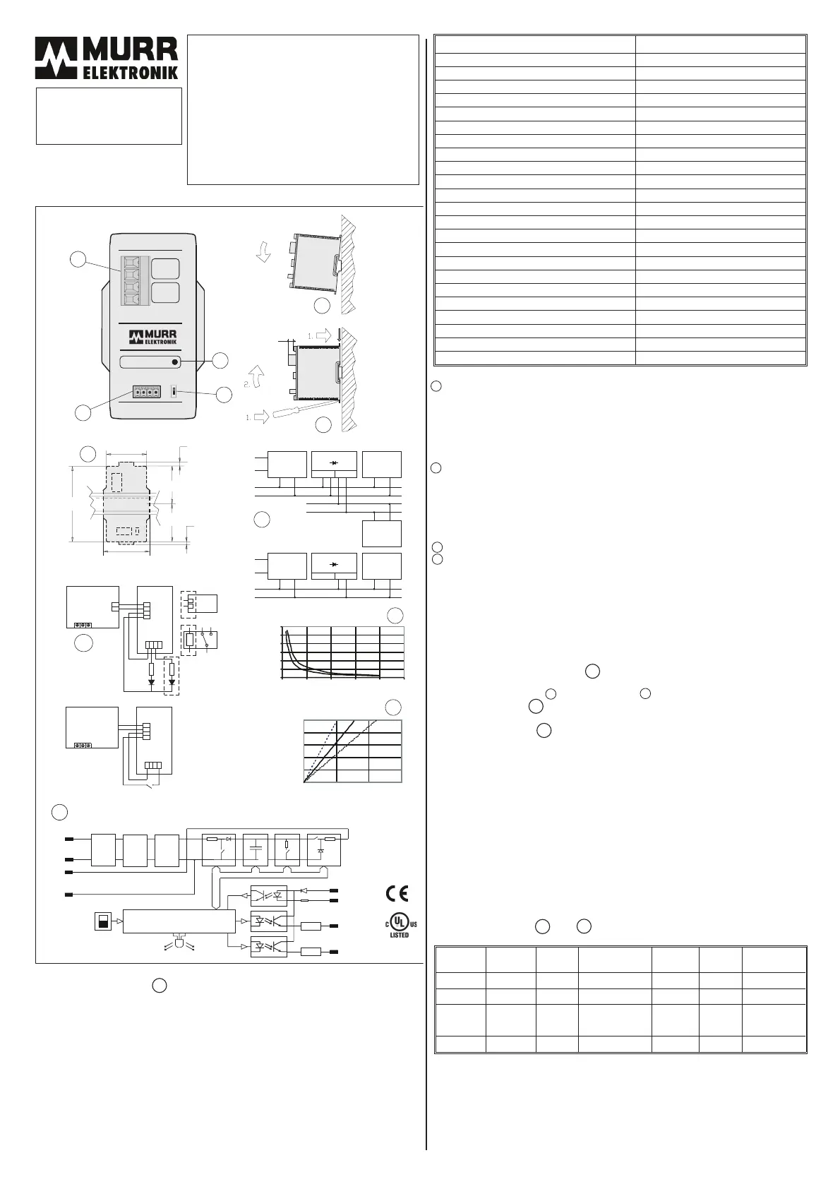
1. Gerätebeschreibung
Pufferkondensatoren werden unter normalen Bedingungen aufgeladen (in dem sie eine höhere
Spannung verwenden, wird auch die höhe der gespeicherten Energie gesteigert). In Folge
eintretender Störungen der Hauptspannung, wird diese Energie benötigt, um die Verbraucher zu
versorgen. Die Überbrückungszeit für Störungen der Hauptspannung beträgt mehr als 200 ms
mit 20 A Pufferstrom und 24V DC. Den Statistiken zur Folge ist diese Zeit lang genug um mit mehr
als 80% Sicherheit für die ungebrochene Stromversorgung der Verbraucher zu sorgen.
Dieses Produkt ist für die Verwendung in Umgebungen mit Verschmutzungsgrad 2 und
überspannungskategorie II oder I vorgesehen und darf nur in diesen Umgebungen eingesetzt
werden.
3. Ausrüstung
Ausgangs- / Eingangsklemme:
Leitungsart
Starr 4 mm² / 11 AWG
Flexibel 4 mm² / 11 AWG
Flexibel mit Adernendhülse ohne/mit Kunststoffhülse 4 mm² / 11 AWG
Adernendhülse müssen eine Mindestlänge haben
≥ 10 mm
Anzugsmoment: 0,5 - 0,6 Nm / 5 - 7 lb. in.
Bitte Leitungen mit mindestens 60/75°C Temperaturbeständigkeit verwenden.
Signalklemme:
Leitungsart
Starr 0,25 - 1,5 mm² / 23 - 16 AWG
Flexibel 0,25 - 1,5 mm² / 23 - 16 AWG
Flexibel mit Adernendhülse ohne/mit Kunststoffhülse 1,5 mm² / 16 AWG
Adernendhülse müssen eine Mindestlänge haben
≥ 10 mm
Anzugsmoment: 0,4 Nm / 3,5 lb. in.
Bitte Leitungen mit mindestens 60/75°C Temperaturbeständigkeit verwenden.
Puffer Verfahren: A (Uin = -1 VDC (werkseitig eingestellt) oder B (< 22,5 VDC)
Betriebsanzeige: Zweifarbige LED (siehe Tabelle “Betriebszustände”)
4. Einbauart
Das Puffermodul muß so eingebaut werden, daß die Verlustwärme ungehindert abgeführt wird.
Dadurch verbessert sich die Gesamtzuverlässigkeit, und ein fehlerfreier Betrieb wird über einen
längeren Zeitraum gewährleistet. Die Kühlung des Puffermoduls erfolgt durch natürliche
Luftzirkulation. Beim Einbau ist möglichst viel Platz für die Luftzirkulation zu lassen. Es ist zu
beachten, daß die Temperatur oberhalb der Geräte ca. 25°C höher ist als unterhalb. Als
Umgebungstemperatur der Geräte gilt die Temperatur direkt unterhalb des Gerätes. Ist die
Luftzirkulation beschränkt, muß zwangsbelüftet werden. Der Einbauplatz muß den
Bedingungen der EN 60950-1 Punkt 4.7 und 4.6.1 genügen. Gehäuseschutzklasse IP 20 (EN
60529).
5. Einbau, Befestigungslöcher
Die Schiene muß so befestigt werden, daß sie sich beim Ein- oder Ausbau des Gerätes nicht
verdreht. Einbauanweisung , Ausbauanweisung .
6. Inbetriebnahme
Das Puffermodul ist als solches gebrauchsfertig; siehe Anschlußmöglichkeiten im Anhang.
7. Signalanschlüsse
Signalausgänge:
A = Aktiv: niederohmig während des Pufferbetriebs.
R = Bereit: niederohmig wenn Puffer vollständig aufgeladen ist
Strom max. 15 - 20 mA (interne Strombegrenzung), Spannungsabfall 1 - 3,5 VDC.
Signaleingang:
I = Sperrung: fallendes Eingangssignal leitet Geräteabschaltung und Zwangsentladung der
Pufferkondensatoren ein.
Strom 1,5 - 2 mA, sinkend
Signalausgänge und Steuereingang sind Dauerkurzschluss-, Leerlauf- und Überlast- fest.
Anmerkung: Sperrmodus bleibt an für 2 minuten nach aktivierung.
8. Puffer Verfahren / Buffer modes:
Mode A: Eingangsspannung - 1VDC;
Pufferung erfolgt bei Spannungsabfall schneller als 0,5 V/s und mehr als 1 VDC. Die Spannung
wird auf diesem Niveau gehalten.
Mode B: fest 22,5 VDC;
Pufferung ab Klemmenspannung < 22,5 VDC; Spannung wird auf 22,5 VDC gehalten.
9. Betriebszustände und
Betriebs-
zustände
Strom Zeit Status LED Ausgang
‘Aktiv’
Ausgang
‘Bereit’
Puffer
Kondensator
Ladebetrieb < 500 mA 20 - 45 s grün / blinkt 2,5 Hz sperrt sperrt lädt auf
Leerlauf < 85 mA - grün / leuchtet sperrt leitet voll
Pufferbetrieb 0 - 20 A
siehe
Diagramm rot / leuchtet leitet sperrt entlädt
Sperrbetrieb < 85 mA 120 s grün 0,1 s / 1 s sperrt sperrt ist entladen
10. Normen
Sicherheit: EN 60950-1, UL 508, SELV
EMV: EN 61000-6-2
EN 61000-6-3
EN 55022 class B
Änderungen vorbehalten.
Lesen Sie diese Bedienungsanleitung vor
Einbau und Gebrauch des Puffermoduls
aufmerksam durch, damit Sie die
Eigenschaften des Puffermoduls nutzen
können. Das Puffermodul enthält
Eigenschaften, die Ihnen zu mehr
Zuverlässigkeit in Ihrem System verhelfen.
Bewahren Sie diese Anleitung für einen
möglichen späteren Gebrauch auf.
MB Cap 20/24
Art. Nr. 85394
BEDIENUNGSANLEITUNG
2. Technische Spezifikationen, Art. Nr. 85394
V1.2
Nennspannung
24 VDC (SELV / PELV)
Spannungsbereich
23 - 30 VDC
Nennstrom
< 85 mA / Leeflauf, < 500 mA Ladevorgang
Verpolungschutz
ja
Schutz vor Spannungsspitzen
<35VDC
Ladeverzögerung
<100ms
Ladezeit
20 - 45 s
Ladestrom
<500mA
Ausgangsspannung
24 VDC
Spannungsbereich
22 - 28 VDC
Pufferspannung
Uin -1 VDC oder < 22,5 VDC
Nennausgangsstrom
20 A
Strombegrenzung
26 A
Pufferzeit
0,2 s/ 20 A/ 24 VDC - 4 s/ 1 A/ 24 VDC
Leistungsaufnahme
1,7 W / bereit
Wirkungsgrad
>95%/20A
Restwelligkeit
<200mV
rms
Parallelschaltbarkeit
möglich
Relative Feuchtigkeit
5 - 95% , keine Kondensation
Betriebstemperatur
0°C - +55°C
Lagertemperatur
-25°C - +85°C
Gehäuseschutzklasse , Gehäuse, EN 60529
IP 20
Abmessungen B x H x T x TA; Gewicht
62x115x145x20mm; 0,66kg
Ladezeit
Ladezustand
Ladezeit / s
min. typ. max.
100%
80%
60%
0%
40%
20%
020
40
0
1
2
3
4
5
6
0 5 10 15 20 25
Pufferzeit
Zeit /s
min.
typ.
5
6
8
7
11
54
115
2
57
58
5
62
1
2
3
4
9
12
10
TA
Output
+
-
Ready:
Charging:
20A
+
-
Input
DC 23-30V
ART. NO. 85394
Discharging:
A
R
I
A
BUFFER MODE
R
I
+
GREEN blinking
GREEN continuous
RED
MB Cap
A
B
A Uin-1V
B22.5V
- Inhibit
- Ready
-Active
AC
Ausgang
Eingang
Versorgung
Puffer Gerät/e
Ungepufferte
Lasten
Art. No. 85394
Gepufferte
Lasten
Gepufferte
Lasten
Art. No. 85394
Ausgang
Eingang
> 2kOhm
R > 2kOhm
+ARI
Versorgung
Puffer Gerät/e
DC - nicht Stabilisiert
DC - Stabilisiert
AC
+
+
DC - Stabilisiert
Programmierbare
Steuerung
Eingang
GND
Spulenwiderstand
Relais
+ARI
+
+
R
AC
Versorgung
LED
AC
ON/OFF
Puffer
Gerät
LNPE
LNPE
+
+
-
-
-
-
-
-
+
-
+
-
+
-
+ -+ -
+
-
+
-
+
+
-
-
+
-
Versorgung
Puffer
Gerät
Verpolungs-
schutz
Einschalt-
strom-
begrenzer
Entkopplung
Gepuffert/
Ungepuffert
Ladegerät Puffer-
kondensator
Puffer-
kondensator
Abschaltung
Puffern
Eingang
Ausgang
Schwellspannungs
Einstellung
Steuerelektronik
Ein-/Ausgangsspannungs
Kontrolle
Uin-1V
22.5V
Strom-
begrenzung
Strom-
begrenzung
15mA
15mA
15kohm
rot
grün
Zustandsanzeige
Max. 35VDC
Sperrung
+
Active
Bereit
0
525
20
10
15
Strom / A
0
1
2
3
4
5
6
E222272
1VD7
IND.CONT.EQ
10
1
2
3
4
7
5
6
8
9
11
12