2017 Microchip Technology Inc. DS20005713B-page 1
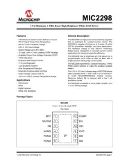
MD1213
Features
• 6 ns Rise and Fall Time with 1000 pF Load
• 2A Peak Output Source and Sink Currents
• 1.8V to 5V Input CMOS Compatible
• 4.5V to 13V Total Supply Voltage
• Smart Logic Threshold
• Low-Jitter Design
• Two Matched Channels
• Outputs can Swing Below Ground
• Low-Inductance Package
• Thermally Enhanced Package
Applications
• Medical Ultrasound Imaging
• Piezoelectric Transducer Drivers
• Non-Destructive Testing
• PIN Diode Driver
• CCD Clock Driver/Buffer
• High-Speed Level Translator
General Description
The MD1213 is a high-speed dual-MOSFET driver. It is
designed to drive high-voltage P-channel and
N-channel MOSFETs for medical ultrasound and other
applications requiring a high-output current for a
capacitive load. The high-speed input stage of the
MD1213 can operate from 1.8V to 5V logic interface
with an optimum operating input signal range of 1.8V to
3.3V. An adaptive threshold circuit is used to set the
level translator switch threshold to the average of the
input logic 0 and logic 1 levels. The input logic levels
may be ground referenced even though the driver is
putting out bipolar signals. The level translator uses a
proprietary circuit, which provides DC coupling
together with high-speed operation.
The output stage of the MD1213 has separate power
connections enabling the output signal L and H levels
to be chosen independently from the supply voltages
used for the majority of the circuit. As an example, the
input logic levels may be 0V and 1.8V, the control logic
may be powered by +5V to –5V, and the output L and
H levels may be varied anywhere over the range of –5V
to +5V. The output stage is capable of peak currents of
up to ±2A, depending on the supply voltages used and
load capacitance present.
The OE pin serves a dual purpose. First, its
logic H level is used to compute the threshold voltage
level for the channel input level translators. Second,
when OE is low, the outputs are disabled with the A
output high and the B output low. This assists in
properly pre-charging the AC coupling capacitors that
may be used in series in the gate drive circuit of an
external PMOS and NMOS transistor pair.
Package Type